Saturday, November 30, 2013
MC3479 Stepper Motor Driver

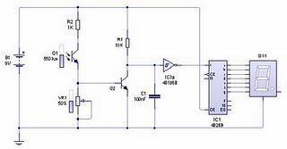
The circuit diagram is given here is a motor controller driver using the Motorola MC3479. The MC3479 is designed specifically for driving a stepper motor phase 2 in bipolar mode and is available in standard DIP and surface mount IC packages.The is compatible with TTL and CMOS and has selectable HI / LOW output impedance .
The output can deliver up to 350 mA each of the two coils of a stepper motor 2 phases. The change of output state occurs in the low to high transition of the input clock pulse. The new output will depend on the exit of age and state of the digital inputs. The output L1 to L4 are the results of high currents, which when connected to a stepper motor a two-phase full-bridge two formations.
Resistors R1 and Rb, Zener diode D1 and IC2 MC14049UB are additional components that are used in the circuit. R1 is an uprising and resistance Rb is used to set the maximum output sink. Zener diode D1 provides back emf protection.
Smart Tracker track anything from your child to shoes
The EPE Minder consists of two type- approved transmitter units and a receiver. If either transmitter becomes separated from the receiver, a buzzer in the latter part will sound.
The receiver is fitted with a switch to allow the use of only one transmitter if required.
MIND HOW YOU GO
This system was originally designed as a two-channel child alarm (to protect either a single child or two children at the same time) but many other applications spring to mind. For example, one transmitter could be placed inside a briefcase and another in a coat pocket. If the user forgot to pick up either of these items and walked away, the buzzer would sound in the receiver. The receiver must be carried on the per- son in a way that would make it practically impossible to lose it. This could be done using a belt clip, for example. Note that it will not be possible to use this system if either the transmitter or receiver were placed inside metal containers or if there were substantial metallic “screening” objects between them.
OPERATING RANGE
The operating range may be adjusted according to the intended purpose. However, it does depend on conditions. Adjustment is carried out by means of “aerial link wires” on the circuit panels. With all these in place, the range of the prototype exceeds 12 metres in open air. It will also work throughout several rooms indoors if required. If the battery voltage in either transmit- ter or receiver falls below a certain value, or if a transmitter is switched off, a buzzer will sound. The specified batteries in the transmitters should provide several hun- dred hours of operation. Those in the receiver should provide around 100 hours.
PERSONAL CODE
The EPE Minder uses a system of digitally encoded low-power radio signals,
which pass from the transmitters to the receiver. The code is different for each transmitter so that the receiver is able to distinguish one from the other. Type-approved, pre-aligned transmitter and receiver modules that operate at 433MHz. are used. No traditional “radio” skills are needed and no licence is needed for their use in the UK.
TRANSMITTER CIRCUIT
The circuit diagram for a single trans- mitter unit is shown in Fig.1. Current is
supplied to the circuit from a 3V “coin” cell, B1, via on-off switch S2 and diode D1. The diode provides reverse-polarity protection. It is best to use the specified Schottky device which introduces a smaller forward voltage drop, and therefore less loss, than a conventional silicon diode (0·2V rather than 0·7V approximately). Capacitor C2 provides a small reserve of energy and pre- vents the supply voltage from fluctuating. This stabilises operation. A low power 7555 timer, IC1, is set up in a standard astable (pulse generator) con- figuration. While switched on, this produces a continuous train of on-off pulses at its output, pin 3.The choice of resistors R1, R2 and capacitor C1 provide one pulse per second for one of the transmitters (Unit A) and one pulse every 1·2 seconds for the other one (Unit B). In fact, the timings are slightly longer but it helps to consider them as above. Also, the on times are much longer than the off ones in each case. The purpose of this will be explained presently.
RECEIVER CIRCUIT
Receiver module, IC1, requires a supply of between 4·5V and 5·5V. The 6V nomi-
nal battery pack, B1, is brought within range by the forward drop of diode D5
(0·7V approx.) This diode also provides reverse-polarity protection. Capacitor C4 charges up and provides a small reserve of energy. This will be useful when the battery is nearing the end of its operating life. When the supply voltage falls below some 4V, the receiver stops working and the buzzer will sound. Below around 3V, the buzzer itself will not operate so it is important to check operation each time the units are used. Receiver IC1 should be of the a.m. (amplitude modulation) type as specified in the components list. As such, it will respond to the on-off pulses provided by the transmitter. The inexpensive super regenerative (rather than superhet) variety will be perfectly adequate. The low-power variants of these receivers have not been tested. Although for battery operation they would appear to be ideal, the standard type is more readily available.
The receiver may be considered as hav- ing separate r.f. (radio frequency) and a.f. (audio frequency) sections. These have individual supply inputs (pins 1, 10, 12 and 15 with some being duplicated). These are all connected together and decoupled using capacitor C1.
TESTING
Having completed the Receiver board, we can now commence testing all three
boards. It helps to minimise the Receiver “hold-off” time by adjusting preset VR1 fully anti-clockwise (as viewed from the left-hand side of the p.c.b.) and preset VR2 fully clockwise (as viewed from the right- hand side of the p.c.b.). Check that the Test link has been left unconnected to prevent IC4b signal from passing to transistor TR1’s base. Switch on Single Channel switch S3 so that Channel A is enabled. With On-Off switch S4 off, insert the batteries. Switch on. After a short delay, the buzzer WD1 should sound. Now place Transmitter A approximately
three metres away from the Receiver, insert the battery and switch on. The buzzer should begin to bleep every second. The same procedure is now repeated for Transmitter B. To do this, switch S3 off to disable Channel A and firmly twist together the ends of the Test link wires. It is not advisable to solder this connection unless the i.c.s are removed first. The buzzer should bleep at a slightly slower rate than for Transmitter A. It is unlikely that the time periods of the two transmitters will be the same (due to overlapping component tolerances).
However, if they are, one of them will need to be changed. Choose slightly higher values for resistors R1 and R2 to slow it down and vice versa. Remove the i.c.s before making any modifications.
HOLD-OFF TIME
When both transmitters have been test- ed, switch S3 on to enable both channels. presets VR1 and VR2 should now be adjusted to approximately mid-track posi- tion. This should provide a sufficient “hold off” time plus a small margin. The buzzer should now remain off and only sound when one of the transmitters is switched off or moved out of range. Leave them operating for several minutes. If the occasional spurious bleep is heard, increase the settings of VR1/VR2 to pre- vent this happening.
Read More..
The receiver is fitted with a switch to allow the use of only one transmitter if required.
MIND HOW YOU GO
This system was originally designed as a two-channel child alarm (to protect either a single child or two children at the same time) but many other applications spring to mind. For example, one transmitter could be placed inside a briefcase and another in a coat pocket. If the user forgot to pick up either of these items and walked away, the buzzer would sound in the receiver. The receiver must be carried on the per- son in a way that would make it practically impossible to lose it. This could be done using a belt clip, for example. Note that it will not be possible to use this system if either the transmitter or receiver were placed inside metal containers or if there were substantial metallic “screening” objects between them.
OPERATING RANGE
The operating range may be adjusted according to the intended purpose. However, it does depend on conditions. Adjustment is carried out by means of “aerial link wires” on the circuit panels. With all these in place, the range of the prototype exceeds 12 metres in open air. It will also work throughout several rooms indoors if required. If the battery voltage in either transmit- ter or receiver falls below a certain value, or if a transmitter is switched off, a buzzer will sound. The specified batteries in the transmitters should provide several hun- dred hours of operation. Those in the receiver should provide around 100 hours.
PERSONAL CODE
The EPE Minder uses a system of digitally encoded low-power radio signals,
which pass from the transmitters to the receiver. The code is different for each transmitter so that the receiver is able to distinguish one from the other. Type-approved, pre-aligned transmitter and receiver modules that operate at 433MHz. are used. No traditional “radio” skills are needed and no licence is needed for their use in the UK.
TRANSMITTER CIRCUIT
The circuit diagram for a single trans- mitter unit is shown in Fig.1. Current is
supplied to the circuit from a 3V “coin” cell, B1, via on-off switch S2 and diode D1. The diode provides reverse-polarity protection. It is best to use the specified Schottky device which introduces a smaller forward voltage drop, and therefore less loss, than a conventional silicon diode (0·2V rather than 0·7V approximately). Capacitor C2 provides a small reserve of energy and pre- vents the supply voltage from fluctuating. This stabilises operation. A low power 7555 timer, IC1, is set up in a standard astable (pulse generator) con- figuration. While switched on, this produces a continuous train of on-off pulses at its output, pin 3.The choice of resistors R1, R2 and capacitor C1 provide one pulse per second for one of the transmitters (Unit A) and one pulse every 1·2 seconds for the other one (Unit B). In fact, the timings are slightly longer but it helps to consider them as above. Also, the on times are much longer than the off ones in each case. The purpose of this will be explained presently.
RECEIVER CIRCUIT
Receiver module, IC1, requires a supply of between 4·5V and 5·5V. The 6V nomi-
nal battery pack, B1, is brought within range by the forward drop of diode D5
(0·7V approx.) This diode also provides reverse-polarity protection. Capacitor C4 charges up and provides a small reserve of energy. This will be useful when the battery is nearing the end of its operating life. When the supply voltage falls below some 4V, the receiver stops working and the buzzer will sound. Below around 3V, the buzzer itself will not operate so it is important to check operation each time the units are used. Receiver IC1 should be of the a.m. (amplitude modulation) type as specified in the components list. As such, it will respond to the on-off pulses provided by the transmitter. The inexpensive super regenerative (rather than superhet) variety will be perfectly adequate. The low-power variants of these receivers have not been tested. Although for battery operation they would appear to be ideal, the standard type is more readily available.
The receiver may be considered as hav- ing separate r.f. (radio frequency) and a.f. (audio frequency) sections. These have individual supply inputs (pins 1, 10, 12 and 15 with some being duplicated). These are all connected together and decoupled using capacitor C1.
TESTING
Having completed the Receiver board, we can now commence testing all three
boards. It helps to minimise the Receiver “hold-off” time by adjusting preset VR1 fully anti-clockwise (as viewed from the left-hand side of the p.c.b.) and preset VR2 fully clockwise (as viewed from the right- hand side of the p.c.b.). Check that the Test link has been left unconnected to prevent IC4b signal from passing to transistor TR1’s base. Switch on Single Channel switch S3 so that Channel A is enabled. With On-Off switch S4 off, insert the batteries. Switch on. After a short delay, the buzzer WD1 should sound. Now place Transmitter A approximately
three metres away from the Receiver, insert the battery and switch on. The buzzer should begin to bleep every second. The same procedure is now repeated for Transmitter B. To do this, switch S3 off to disable Channel A and firmly twist together the ends of the Test link wires. It is not advisable to solder this connection unless the i.c.s are removed first. The buzzer should bleep at a slightly slower rate than for Transmitter A. It is unlikely that the time periods of the two transmitters will be the same (due to overlapping component tolerances).
However, if they are, one of them will need to be changed. Choose slightly higher values for resistors R1 and R2 to slow it down and vice versa. Remove the i.c.s before making any modifications.
HOLD-OFF TIME
When both transmitters have been test- ed, switch S3 on to enable both channels. presets VR1 and VR2 should now be adjusted to approximately mid-track posi- tion. This should provide a sufficient “hold off” time plus a small margin. The buzzer should now remain off and only sound when one of the transmitters is switched off or moved out of range. Leave them operating for several minutes. If the occasional spurious bleep is heard, increase the settings of VR1/VR2 to pre- vent this happening.
Friday, November 29, 2013
Smoke Detector Alarm Using RE46C140
Using the RE46C140 circuit can be designed a very simple smoke detector alarm using few external electronic components . The RE46C140 IC is a low power CMOS photoelectric type smoke detector IC that will provide all the required features for a photoelectric type smoke detector project . This smoke detector alarm design incorporates a gain selectable photo amplifier for use with an infrared emitter detector pair. An internal oscillator strobes power to the smoke detection circuitry for 100us every 10 seconds to keep standby current to a minimum. If smoke is sensed the detection rate is increased to verify an alarm condition.
Smoke Detector Alarm Circuit Diagram

An interconnect pin allows multiple detectors to be connected such that when one units alarms, all units will sound. In standby the LED is pulsed on for 10mS every 43 seconds . In a local alarm condition or the push to test alarm the LED pulse frequency is increased to once every 5 seconds. In the case of a remote alarm the LED not active. In the timer mode of operation the LED is pulsed on for 10mS every 10 seconds.
A comparator compares the photo amp output to an internal reference voltage. If the required number of consecutive smoke conditions is met the device will go into local alarm and the horn will be active. The bidirectional IO pin allows interconnection of multiple detectors. In a local alarm condition this pin is driven high immediately through a constant current source. Shorting this output to ground will not cause excessive current. The IO is ignored as an input during a local alarm. This smoke detector circuit must be powered from a 9 volt DC power supply .
Smoke Detector Alarm Circuit Diagram
A comparator compares the photo amp output to an internal reference voltage. If the required number of consecutive smoke conditions is met the device will go into local alarm and the horn will be active. The bidirectional IO pin allows interconnection of multiple detectors. In a local alarm condition this pin is driven high immediately through a constant current source. Shorting this output to ground will not cause excessive current. The IO is ignored as an input during a local alarm. This smoke detector circuit must be powered from a 9 volt DC power supply .
High HiFi Power Amplifier with MOSFET
Circuit amplifier "High Power HiFi Power Amplifier With MOSFET" is capable of giving the output power to the load speakers 240Watt and 380Watt 8Ohm to load 4Ohm speakers.
Voltage source to a series of power amplifiers "High Power HiFi Power Amplifier With MOSFET" This is a CT 25V 50V 25V to 50V CT of transformer CT. In making this power amplifier needs to be installed heatsinks on the power amplifier (MOSFET) in order to avoid excessive heat. The series of power supply to power amplifer can use the transformer 5A-20A and 35A mounted diode bridge and capacitors for a minimum of 2x 10.000uF electrolit. Details for the power amplifier circuit can be seen in the following figure.

High Power Series HiFi Power Amplifier With MOSFET can modify to increase power output by doubling the final power amplifier is based on the diiginkan. Power generated from doubling the final power amplifier will also double its power output of power amplifier circuit "High Power HiFi Power Amplifier With MOSFET" it.
Simple accu charger circuit

Accu charger circuit is very simple and easy to make, because it only requires a few components are also not more than 10 components. Besides easy charger circuit is also very cheap and very efficient.
This circuit requires power supply from a transformer that comes from an AC voltage 220 and diuturunkan be 12-13 volts and then enter to-circuit and 12 Volt DC output allows for charging 12V battery
| Simple charger schematics |
Thursday, November 28, 2013
Power Amplifier for Audio Laptop
Frequently, the sound yield from a laptops fabricated-in speakers is flat. A capacity intensifier is needed to get an elevated volume. Here is an effortless circuit to intensify the laptops sound yield.
The circuit is constructed around capacity enhancer IC LA 4440 (IC1) and a few alternate parts. LA4440 is a double channel sound capacity speaker. It has level twisting over a vast run of flat to towering frequencies with exceptional channel detachment. Inbuilt double channels prepare it for stereo and extension speaker provisions.
image : http://circuitschematicelectronics.blogspot.com/2011/02/2-x-20-watt-car-amplifier.html
In double mode LA4440 gives 6 watts for every divert and in scaffold mode 19-watt yield. It has swell denial of 46 dB. The sound impact might be grasped by utilizing several 6-watt speakers. Associate binds 2, 6 and ground of IC1 to the stereo jack which is to be utilized with the laptop. Collect the circuit on a customary-reason PCB and encase in a suitable bureau. The circuit works off managed 12V capacity supply. It is suggested to utilize sound enter socket in the circuit plank. Utilize a decent hotness-sink for LA4440.
IR Infra Red Sensor with 7 Segment Display
Infrared light has a difference with ordinary light in general. We can see clearly when a light or light on an object.
As with the infrared light we can not see the manifestation of these rays. Frankly I can not answer when asked why the infrared rays are not visible in the eyes of us. So at night do not hope you can make light by using infrared light. One thing that is often heard from many people that infrared light can utilized for the functions of a camera that can see in dark conditions is often called an infrared camera.Actually I have explained the working principles of electronic circuit section in this blog is about the basic working principle of a series of infrared sensors are simple. To design this sensor circuit you should not find trouble if you ever make another series of sensors. Its just that the sensor circuit consists of the transmitter and receiver, to learn the basic principles of this series of infrared you can see in the Basic Principles Series Infrared Transmitter and Receiver. In the circuit this time I try to utilize the output of this sensor circuit as a trigger circuit counter or counters.
Picture series of infrared sensors | infrared sensor circuit scheme
Component List:
1. Resistors: R1 (33K), R2 (1K), VR1 (Potensio 100K)
2. Capacitors: C1 (100nF)
3. Transistors: Q2 (BC547 should)
4. Photo transistor: Q1
5. IC: 40 106 (Schimitt trigger), 4026 (Decade counter)
6. 7-Segment
WORKING PRINCIPLE:
In the transmitter circuit arrangement so that our task is only an infrared LED lights up and no shortage or excess of power, therefore, use 680 ohm resistors. On The set of photo transistor receiver serves as a useful tool sensor sensed a change in the intensity of infrared light. When infrared light is not on the photo transistor, the photo transistor is like a switch is open so that the transistor is in cutoff position (open). Because the collector and emitter open it in accordance with the laws of the voltage divider, the collector emitter voltage equal to supply voltage (logic high). The output of these collectors would make a series of counter counting irregularly if we did not dampen the bounce output to the input couinter. To reduce the bounce and clarify the logic signal to be our input to counter circuit, we use Schmitt trigger ignition. Schmitt trigger ignition is very useful for those of you who relate to digital circuits, eg, using the damping bounce of mechanical switches on the input digital circuit.
The series of counters that I use here is to use IC 4026 (Decade Counter), one of the family ic CMOS. IC counter counts up if this will get the clock input changes from logic low to high. This IC can directly connect it to the seven segment because the output is designed for seven segment mmang. So you do not need to use as a modifier decoder IC binary value into a score of 7-segment.
To menmgatur you can rotate the sensor sensitivity potensio VR1 at a critical point, or if necessary you can replace R2 with a more appropriate value.OTL 100W Power Amplifier 2N3055
This is Circuit Power Amp OTL 100W Amplifier by transistor 2N3055. It easy to build because normal circuit power amp OTL. To use power supply 98V 5A. Out put power 100W at Speaker 8 OHM or 120W : 4OHM.
Read More..
![OTL 100W Power Amplifier [2N3055]](https://blogger.googleusercontent.com/img/b/R29vZ2xl/AVvXsEiedRw6_0H2NMCr3hUZ27ms1NcOLpcC8pYetxznCJK2VdAEci0Ftpn3_ANk7-5HF8U6ZPFB-7dqVGEGN8ZAotw6aR5P0KSRfXRwKxPyrURlB24JKSqUNQ-ZLqA17YXfFt2ehTvkd5O5AH6j/s400/OTL+100W+Power+Amplifier+%5B2N3055%5D.jpg) |
| OTL 100W Power Amplifier [2N3055] |
Wednesday, November 27, 2013
Emergency Lights Circuit
The series of emergency lights on this one is a series of emergency lighting is quite simple and not difficult to make.
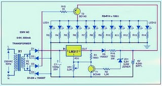
Frankly this circuit is not my own design, but at least this series can add to your collection of electronic circuits. The circuit is actually almost the same as the battery charger circuit, its just that in this emergency coupled switching circuit as a circuit breaker when the circuit load is connected to the supply voltage of 220 volts or in other words on the charging position. Meanwhile, when the voltage of 220 volts is lost (PLN lights off), then automatically switches the load switching circuit and turn on emergency lights, where the supply that is used is derived from batteries that have been installed in stand-by position.
In a series of emergencies over the use of LED as a lighting load emergency. And indeed these days we find a lot of emergency lights that are sold in the market that use LEDs, but the LED is used instead led carelessly but has led a gleam of light. The advantages of the use of this led the led is very efficient because once will consume battery power so that with a limited supply to run the series in a long time.
Circuit components used for emergency lighting is not too much, and indeed the components used are the components that are commonly used as components for circuit switching power supply and battery charging. IC LM 317 ic regulator is useful as a producer of supply voltage to supply the batteries. Transistor T2 (BD 140) is useful as switching, ie, decide the flow toward the load at 220 volts PLN lamp life so that lighting will be extinguished. But when the lights PLN did not provide the supply voltage of the transistor T2 will connect the connection from the battery to the load light.
Components used:
Resistors: R1 (180 uhm), R2 (1.2 K), sd R3 R14 (100 ohms), R15 (1 K) and R16 (16 ohm, 5 watt)
Capacitors: C1 (1000 UF)
Diodes: D1 until D5 (IN 4007)
Transistors: T1 (BC 548) and T2 (BD 140)
Zener Diodes 6.8 Volt
IC: LM 317
Battery charger
Transformer
If you are not happy using this type of charger with IC LM317 series like the example above then you can use another type of charger circuit that you think is more appropriate and can work optimally. Then you simply add the switching function by using one or more transistors.
2 X 1 8 Watt stereo low power amplifier circuit
This is Low power amplifier , based on IC TDA2824 product of Philips. Maximum output is about 2 X 1,8 Watt , these include low output amplifier type. Minimum required voltage 3 Volts and maximum voltage of 18 volts DC.

Spec :
- Supply Voltage : 3 - 18 Volts
- Power Output : 2 x 1,3 Watts
- RL impedance : 4 Ohms
- Frequency responses : 30Hz -18kHz
- Quiescent current : 6 mA
Tuesday, November 26, 2013
BA5406 10W Stereo Power Amplifier
BA5406 is a monolithic integrated stereo amplifier from ROHM semiconductors. It can transfer 5W apiece channel into a 4 ohm loudspeaker by the side of 9V supply. Amplifiers based on BA5406 does not require an output coupling transformer and can subsist operated from a single supply. The operating voltage range is from 5 to 15V DC. This makes the IC correct in lieu of low power car audio applications. Other applications of BA5406 are portable audio players, stereo module systems, television and all that. The BA5406 has important channel separation, excellent channel isolation, unimportant pop-up clatter, low noise, low thermal resistance and is open arrived a 12 pin SIP package.
 |
| BA5406 10 Watt Stereo Power Amplifier |
In the circuit diagram revealed lower, BA5406 is configures to hand over 5×2 watts into 4 ohm loudspeakers by the side of a supply voltage of 9 volts. Capacitor C3 is a power supply filter capacitor. C11 and C12 are input DC decoupling capacitors on behalf of the missing and due channels. C3 and R2 forms a Zobel arrangement for the not here output while C6 & R3 forms the same for the right channel. single-mindedness of the Zobel network is to reduce oscillations and rally in height frequency stability of the amplifier. Potentiometers R5 and R6 serves since the volume control on behalf of the not here and right channels. CapacitorsC4 and C8 pair the outputs of the amplifier to the speakers. C9 and C10 are clamor filtering capacitors. C1 and C5 are bootstrap capacitors for the not here and right channels.
Bass Booster with TL072
The following is megabass circuit schematic (rangkaian megabass) . The megabass circuit is a modified Baxandall tone control with no bass cut and no treble control. It boosts frequencies from about 30Hz to 160Hz can boost by 14dB.
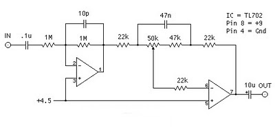
Note:
The input capacitor can be replaced with a .01uf cap if you wish.
The 10pf capacitor is optional and will start rolling off everything over 15kHz. 5pf will double this to 31kHz.
The tone control requires a low impedence input. If you already have a low impedence input, the input buffer can be removed. However, the output is inverted.
The opamp is not critical. A 4558 would be just fine.
I do not show the parts for the +4.5 reference. Here is the +4.5 voltage divider I used.
IC A4558 Pinning
The A4558 is a monolithic Integrated Circuit designed for dual operational amplifier.
Absolute maximum ratings of A4558 Ap-amp
Supply voltage VCC 20 or ±10 V
Differential input voltage VIND 20 V
Input voltage VIN ±10 V
Power Dissipation PD 300 mW
Operating temperature Topr -45 ~ +85 °C
Storage temperature Tstg -55 ~ +150 °C
Read More..
Bass Booster Schematics
Note:
The input capacitor can be replaced with a .01uf cap if you wish.
The 10pf capacitor is optional and will start rolling off everything over 15kHz. 5pf will double this to 31kHz.
The tone control requires a low impedence input. If you already have a low impedence input, the input buffer can be removed. However, the output is inverted.
The opamp is not critical. A 4558 would be just fine.
I do not show the parts for the +4.5 reference. Here is the +4.5 voltage divider I used.
IC A4558 Pinning
The A4558 is a monolithic Integrated Circuit designed for dual operational amplifier.
Absolute maximum ratings of A4558 Ap-amp
Supply voltage VCC 20 or ±10 V
Differential input voltage VIND 20 V
Input voltage VIN ±10 V
Power Dissipation PD 300 mW
Operating temperature Topr -45 ~ +85 °C
Storage temperature Tstg -55 ~ +150 °C
50W car audio amplifier schematic circuits
 Car power amplifier uses SI1050GL IC as the main amplifier. The output power 50 Watt 8 ohm mono impedance. Up to 25 Volt DC voltage. with source voltage of this amplifier car battery has to work.
Minimum of 12 Volt battery voltage, less than a sound or audio is issued less than the maximum and less good. You can assemble this circuit amplifier with a schema like this.

Part List
R1 = 100K
R2 = 1R
C1 = 2.2uF
C2 = 22uFC3 = 100uF
C4 = 0.1uF
C5 = 100uFU1 = SI1050GL
If you want to make stereo amplifier , you must required multiply the two of components.
Monday, November 25, 2013
TV Remote Tester Circuit
The circuit is very effective to test the remote controls what still works or not, the remote record will be tested using infra red. Examples of the TV remote, AC and others. Please try I am sure 100% will be successful.
 |
| TV Remote Tester Circuit |
The workings of the circuit is very simple, when the infra red sensor receive infrared signals pin 2 sensor will produce a voltage, this voltage will drives the PNP transistor so that the LED lamp and piezo disc (BZ) is active. for the power supply you can use a 9 volt battery and then use IC 7805 or use 1.5 volt batteries x 3
Following the specification of components installed
Transistor BC557
TSOP 1738 Sensor Infra Red
R1 = 10k ohm ¼ watt Resistor
R2 = 1k ohm ¼ watt Resistor
R3 = 1k ohm ¼ watt Resistor
BZ = piezo disc
led
Power amplifier 450W with sanken
Circuit of power amplifiers with power output of 450 watts mono , amplifiers are also frequently used in the amplifier a high-power amplifier, which used in an event, in the field and the placed closed. Because this amplifier suitable for the woofer, fullrange speaker, and can also be fixed for the subwoofer speaker. To further strengthen and maximize the amplifier ,its power supply circuit also must be accurate, for electrolytic capacitors in power supply ,voltage capacitors use 80V or more, and a capcity 20000uF upwards, so when the bass amplifier is high , the voltage is not lot of experience dropping. Diode bridge use a minimum of 35A, or adjust the current input voltage. If the power supply has fulfilled the desire, the supply to the power amplifier.In the buffer circuit uses PNP transistor A1266 / A564 / A733 /A1015 / A798 and NPN with MJE340.To the driver circuit using PNP transistor MJE350 and MJE350. For the final amplifier circuit use two set 2SC2922 and 2SA1216. Use a quality sanken transistor to maximize quality sound output.Below is the amplifier and finshed PCB layout.


 |
| bottom view |
 |
| Top view |
If the track pcb does not look, you can download this series in the form of fort board, use the eagle cadsoft application to open it, but its components are not ordered , to their own satisfaction you can design it with your whishes.
Download file .brd here
 |
| Installation power amplifier |
 |
| This is power supply |
 |
| already amplifier |
Schematic Audio Amplifier with IC AN313
This schematic very suitable applied on small speakers. Because the maximum output is 3W and the minimum voltage is 12 Volt , this will make speaker does not damage quickly. If you use speaker with impedance 8 Ohm , you must make parallel circuit speaker dont use series circuit.
See This Schematic and datasheet IC AN313 below :

Datasheet IC AN313
Vcc = 12-20 V
Pout = 2x3 W
RL = 8 Ohm
Ft = 40hz -18Khz
Icco = 40 mA
Package = TABS6-16
Manufactered = MATSUSHITA
Or you can call, Datasheetnya IC AN313
Sunday, November 24, 2013
Schematic Audio Amplifier with IC AN7102S
This Schematic use IC AN7102S , this is setereo amplifier and have output speaker 7,5 mW with impedance 32 Ohm . Supply need 1Volt to 3 Volt , wow this amplifier low voltage. You can use this amplifier on radio is use battery . With just one battery with voltage 1,5 Volt you can play this amplifier.
See this Schematic below :
 |
| Click to Enlarge |
Datasheet IC AN7102S
Vcc = 1-3 V
Pout = 2X 7,5 mW
RL = 32 Ohm
Ft = 20hz - 20Khz
Icco = 7 mA
Package = DIP-18
Manufactered = MATSUSHITA
Mosfet Power Amplifier 100 Watt
At this time a unsophisticated MOSFET amplifier or else power Amp which Output power is plus/minus 100 Watt/RMS with 8 Ohms otherwise ohter plus/minus 160 Watts /RMS with 4 ohms.
 |
| Mosfet Amplifier 100 Watt RMS |
Regarding this circuit simplicity, The distortion is plus/minus 0.1 %. In support of mob-width -3 db(decibel) is increase for 4 Hz to 96 Khz, it is narrow by C1, R1, C2 and R2. Taking part in the two transistors are T1 and T2 makes a initial differential stage part, So,current source(I) of +/- solitary mA is put with resistor R3. In favor of the upgraded project, The current source(I) is new efficient in stability. Coil P1 allows a fine tuning of dictate current voltage on amplifier’s output. Place the Coil P1 with it’s partially usefulness in favor of first power up, so therefore break it unhurriedly for a lowest DC output voltage. custom a essential quality compoment.
Electronic Part
C1 = 2,2 µF MKP, MKT 100 in opposition to
C2 = 330 pF céramique 50 V
C3 = 100 nF MKP, MKT 100 in opposition to
C4 = 100 µF 40 V électro-chimique
C5, C6 = 18 pF céramique 50 vs.
C7 = 100 nF MKP, MKT 250 V (C8 = 47 µF 100 V)
R1, R3 = 47 K (R3 = 330 -> 470 Ohms)
R2 = 2K2
R4, R5 = 3K9
R6 = 1 K
R7 = 27 K
R8, R9, R11 = 100 ohms
R10 = 10 K
R12, R13 = 470 ohms
R14, R15 = 0.33 ohms 5 watts
R16 = 10 ohms 3 watts (R17 = 1 K R18, R19 = 10K)
T1, T2, T9,T10 = 2SD756A,2SD716A, BC556B (attention au brochage différent - take be concerned representing pin arrange)
T7 = IRFP240, 2SK1530, 2SJ162, BUZ900DP, BUZ901DP (attention au brochage dissimilar - take care for pin layout : GDS GSD)P1 = 100 ohms (25 turns - 25 turns)
Saturday, November 23, 2013
Schematic Audio Amplifier with IC AN5265
Schematic Description :
This Circuit Require voltage 12 -26 Volt. Good Voltage use is 16 Volt , Because its not too small and not too big Voltage. If use voltage that is to large it will quickly damage the IC. And if use voltage that is to small it will make less than maximum sound output.
See this Circuit and datsheet IC AN5265 Below :
 |
| Click to Enlarge |
Datasheet IC AN5265
Vcc = 12-26 V
Pout = 2,3 W
RL = 16 Ohm
Ft = 40hz - 18Khz
Icco = 9,5mA
Package = SIP2-9
Manufactered = MATSUSHITA
Vertical IC PIN OUT DATA
Vertical Vin = input (non-inverted), Vout = Vertical output, VfB = Vertical feedback (inverted inpput)
Vcc to pump-up can be traced through the diode PUM-up and pump up Elco Capacitor
VfB = or to Vin2
= Gnd or Vcc (-)

Vertical IC PIN-OUT DATA
AN5521 Vin = 4, Vout = 2, Vcc = 7, Gnd = 1, VfB =
AN5522 Vin = 7, Vout = 5, Vcc = 2, Gnd = 4, VfB = 1
AN5539 Vin = 4, Vout = 2, Vcc = 6, Gnd = 1, VfB = 5
AN15525 Vin = 7, Vout = 5, Vcc = 2, Gnd = 4, VfB = 1
LA7832 Vin = 4, Vout +2, Vcc = 6, Gnd = 1, VfB = 5
LA7835 = 2 Vin, Vout = 11, Vcc1 = 1, Vcc2 = 7,
LA7837 = 2 Vin, Vout = 12, Vcc1 = 1, Vcc2 = 8, Gnd = 11, VfB = 7
LA7838 = LA7837
LA7840 Vin = 4, Vout = 2, Vcc = 6, Gnd = 1, VfB = 5
LA7841 = LA7840
LA7845 = LA7840
LA7846 = 5 Vin, Vout = 3, Vcc = 7, Gnd = 2, VfB = 6
LA7848 Vina = 5, VinB = 6, Vout = 3, Vcc (+) = 7, Vcc (-) = 2
LA7876 Vina = 5, VinB = 6 Vcc (+) = 7, Vcc (-) = 2
STV9302 = see AN5522
STV9379 = See AN5522
TA8403 Vin = 4, Vout = 2, Vcc = 6, Vcc = 6,
TA8445 Vin = 2, Vout = 11, Vcc1 = 1 (9v), Vcc2 = 7 (26v), Gnd = 10, 50/60 =
TDA1771 Vin = 3, Vout = 1, Vcc = 9. Gnd = 5
TDA4865 Vin = 6, Vout = 5, Vcc = 1, Gnd = 4, VfB = 2
TDA8175 Vin = 7, Vout = 5, Vcc = 2, VfB = 1
TDA3653 Vin1 = 1, Vin2 = 3, Vcc1 = 9, Vcc2 = 6, Vou = 5, Gnd = 4
TDA8350 Vina = 1, VinB = 2, VoutA = 10, VoutB =, Vcc1 = 3, Vcc2 = 9, Ewin = 12, Ewout = 11
See tda8357 TDA8351 =
See TDA8357 TDA8356 =
TDA8357 Vina = 1, VinB = 2, VoutA = 7, VoutB = 4, Vcc1 = 3 (12v), Vcc2 = 6 (45V), Gnd = 5
TDA8358 Vina = 1, VinB = 2, Vcc1 = 3 (12v), Vcc2 = 9 (25V), VoutA = 4, VoutB = 10, Gnd = 6.7, Ewin = 5, Ewout = 8
TDA9302 = see LA78040
Read More..
Vcc to pump-up can be traced through the diode PUM-up and pump up Elco Capacitor
VfB = or to Vin2
= Gnd or Vcc (-)
Vertical IC PIN-OUT DATA
AN5521 Vin = 4, Vout = 2, Vcc = 7, Gnd = 1, VfB =
AN5522 Vin = 7, Vout = 5, Vcc = 2, Gnd = 4, VfB = 1
AN5539 Vin = 4, Vout = 2, Vcc = 6, Gnd = 1, VfB = 5
AN15525 Vin = 7, Vout = 5, Vcc = 2, Gnd = 4, VfB = 1
LA7832 Vin = 4, Vout +2, Vcc = 6, Gnd = 1, VfB = 5
LA7835 = 2 Vin, Vout = 11, Vcc1 = 1, Vcc2 = 7,
LA7837 = 2 Vin, Vout = 12, Vcc1 = 1, Vcc2 = 8, Gnd = 11, VfB = 7
LA7838 = LA7837
LA7840 Vin = 4, Vout = 2, Vcc = 6, Gnd = 1, VfB = 5
LA7841 = LA7840
LA7845 = LA7840
LA7846 = 5 Vin, Vout = 3, Vcc = 7, Gnd = 2, VfB = 6
LA7848 Vina = 5, VinB = 6, Vout = 3, Vcc (+) = 7, Vcc (-) = 2
LA7876 Vina = 5, VinB = 6 Vcc (+) = 7, Vcc (-) = 2
STV9302 = see AN5522
STV9379 = See AN5522
TA8403 Vin = 4, Vout = 2, Vcc = 6, Vcc = 6,
TA8445 Vin = 2, Vout = 11, Vcc1 = 1 (9v), Vcc2 = 7 (26v), Gnd = 10, 50/60 =
TDA1771 Vin = 3, Vout = 1, Vcc = 9. Gnd = 5
TDA4865 Vin = 6, Vout = 5, Vcc = 1, Gnd = 4, VfB = 2
TDA8175 Vin = 7, Vout = 5, Vcc = 2, VfB = 1
TDA3653 Vin1 = 1, Vin2 = 3, Vcc1 = 9, Vcc2 = 6, Vou = 5, Gnd = 4
TDA8350 Vina = 1, VinB = 2, VoutA = 10, VoutB =, Vcc1 = 3, Vcc2 = 9, Ewin = 12, Ewout = 11
See tda8357 TDA8351 =
See TDA8357 TDA8356 =
TDA8357 Vina = 1, VinB = 2, VoutA = 7, VoutB = 4, Vcc1 = 3 (12v), Vcc2 = 6 (45V), Gnd = 5
TDA8358 Vina = 1, VinB = 2, Vcc1 = 3 (12v), Vcc2 = 9 (25V), VoutA = 4, VoutB = 10, Gnd = 6.7, Ewin = 5, Ewout = 8
TDA9302 = see LA78040
8 to 18 volts TDA2005 Power Amplifier
This time, there is a series of audio amplifer 20W as well, but using IC TDA 2005 as a series of his base amplifier. The series of 2x20 Watt Audio Power Amplifier using TDA2005 can you see in the picture below.
Technical Data:
Performance of TDA2005M: (for this circuit); At 4.14 V supply voltage: 2 x 20 watts (stereo) into 4 Ohms.
Distortion: Approx. 0.2% at 4 Watts into 4 ohm load.Frequency Range: Approx. 20 Hz to 22 KHz.
Input Sensitivity: Approx. maximum 150 mV rms. .
Power supply: + 8 to 18 volts, approx. 3.5 Amps maximum per channel.
source [link]
Friday, November 22, 2013
Car power amplifier with TA82010AH
IC TA8210AH is ic often used in amplifiers used in the room, It is suitable for power amplifiers car speakers taht fit and wear ell, surely this amplifier circuit works with a maximum also high quality. Supply voltage is not too high , only 12 VDC and is also good at high current. For high current amplifier power of the stronger . You can use the batteries that have current 10 A or higher . Power output up to 200W stereo with 8 Ohm impedance.
Part List :
R1 =1K
R2 =50K trim
R3 =1K
R4 =50K trim
R5 =680R
R6 =680R
R7 =150K
R8 =2R2
R9 =2R2
R10=2R2
R11=2R2
C1 =1uF
C2 =1uF
C3 =47uF
C4 =47uF
C5 =100n/400V
C6 =220uF
C7 =220uF
C8 =100n/400V
C9 =100n/400V
C10=100n/400V
IC1=TA8210AH
X2-3=in R
X2-2=gnd
X2-1=in L
X1-1,X1-2=Out R
X1-3,X1-4=Out L

Multi channel audio systems
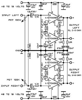
Multi-channel Audio
Multi-channel audio systems are widely used within novel sound campaign. The word “multi-channel audio” process with the intention of, the audio method can transpire accomplished of conduct multiple audio channels (more often than not called audio tracks) to rebuild the sound on a multi-loudspeaker setup.
Usually two digits separated by a decimal (.) end (2.1, 4.1, 5.1, 6.1, 7.1, and the rest.) are used to classify the various kinds of orator fix-up, this total basically depending on how many audio tracks are used. about audio systems solitary suffer a single channel (called monophonic sound otherwise single channel audio) or two channels (stereophonic sound or else 2.0 channel sound)
The initial numeral shows the quantity of primary channels (called satellite units), both of which are reproduced on a single presenter (these speakers are accomplished in place of use the frequency range from 100Hz to 22Khz), while the back up (decimal figure) refers to the presence of LFE (Low Frequency Effect), which is reproduced on a subwoofer.

Tranceiver DC adapter
This DC adaptor provides a regulated 9V source for operating a transceiver in the car .The IC LM317 is mpounting tab is electrically connected to its output pin. so take this into account tour version of the adapter. The LM317T regulator dissipates 2 or 3 Watt in this circuit , so mount it on a 1- x -2 inch piece of 1/8 inch thick alumunium heatsink. Dont forget to give heatsink on the IC LM317.
Thursday, November 21, 2013
FM Moulator with IC 555
FM Modulator circuit is a simple FM modulation circuit using IC 555, where the resulting modulated signal has a tenuous meeting depends on the signal frequency information.

The resulting signal can be spelled out quite nice and stable so that the result will be more perfect. No winding or inductor in series modulator, so you do not need to bother to make a winding and calculate the value of the coil that you created it. With this circuit the desired value of frequency modulation can be obtained easily by calculating the frequency of IC 555 in general, which is determined by the resistor 6.8 K and 3.3 K and 0.1 UF capacitor. To obtain the other frequencies of your stay replace one or all three components.
Actually fm modulator ic 555 circuit is very simple though, but I think it reliable enough to handle a simple application purposes that do not require a big power or a very high frequency. But if you want more power you can add the RF amplifier circuit at the output of this circuit. Thus, the results of modulated signal can be amplified with the help of a series of supporters. In accordance with my experimental series modulators can work well at frequencies below the MHz range, because it is not IC IC 555 which is devoted to support of a very high frequency. You can use oscilltor transistor circuit, XTAL or others if you need a very high frequency.
The difference circuit with IC 555 on the multivibrator circuit in general is the use of pin 5, on the FM Modulator circuit is pin 5 of IC 555 is used as input information signal, which in turn will influence the shape of the output signal (modulated). But in applying this 5 pin multivibrator functions normally associated with 0.01 UF capacitor or left alone.
Simple Circuit 12V to 120V DC DC Converter
 Its a simple circuit of 12V DC to 120V DC converter. The circuit consists of two phases first phase of the investor base and then a rectifier and filter stage. IC1 NE555 is wired as an astable multivibrator operating at a frequency of 100 Hz and can be adjusted to the preset R1. IC1 output is coupled to the clock input of IC2 is a dual CMOS D flip-flop. IC2 divides the pulse train of 100 Hz IC1 2 50 Hz pulse trains that are 180 degrees out of the party and offered on the pin 1 and 2 of IC2.
When pin 1 is high transistor Q1 conducts and current flows through the upper half of T1 primary winding. When pin 2 is the transistor Q2 conducts and high current flows through the lower half of the primary coil T1. As a result of a voltage of 120 V AC are induced in the secondary of T1. This voltage is rectified with bridge D1 to provide a 120V DC output. Capacitor C2 is the DC input filter, while C3, C4 are the output filters.
Notes.
- The circuit can be assembled on a vero board.
- Q1 and Q2 require heat sink.
- Output power of this dc dc converter is around 100 watts.
- IC1 and IC2 are to be mounted on holders.
- An optional 5A fuse can be added in series to the 12V supply line.
- T1 can be a 9-0-9V /250V/3A mains transformer.
- If 3A bridge is not available make one using 1N5408 diodes.
- Out of the two Flip-Flops inside CD4013 only one is used here.
- Output of IC1 must be set to 100Hz by adjusting preset R1
TDA9302 Vertical deflection output schematics
The TDA9302H is a monolithic integrated circuit in HEPTAWATTTM package. This is a high efficiency power amplifier for direct drive vertical rolls from the yokes of TV. This is intended to be used in Color and B & W television as well as in monitors and displays .


Supply Voltage pin 2 35V
Flyback peak voltage 60V
Voltage at pin 3 +Vs
Amplifier Input Voltage -0.5V
Deflection Output Current ± 1.8 A
Pin 3 DC Current at V5 < V2 100 mA
Total Power Dissipation at Tcase 90 °C
Storage and Junction Temperature – 40, +150°C
Part List :
Resistor
R1 = 12K
R2 = 10K
R3 = 27K
R4 = 12K
R5 = 1R
R6 = 330R
R7 = 1.5R
Ry = 5.9R
Capacitor
C1 = 680mF
C2 = 220uF
C3 = 220uF
C4 = 0.22uF
C5 = 1000uF
C6 = 4.7uF
Diode
D1 = BY252
IC = TDA9302H
Subscribe to:
Posts (Atom)