Friday, December 27, 2013
Process formation of RGB signal on TV

Basically the UOC is equipped with RGB or YUV input from external, so it is possible to use the DVD input. Selection of these inputs can be done internally within the IC. But in the G7 and G7A chassis input YUV signal is not used, so in the ground.
RGB signal processing flow is described according to the image below :
 |
| Diagram of the formation RGB signal |
1. Signal Yint, uint, and Vint is derived from a series of color decoder and Y / C switch is fed into a series of YUV selector 1.
2. From YUV selector, sub-carrier signal color (U and V) is inserted into the chain matrix. In this matrix series component sub-carrier signal BY of the color (U signal) and BY component of sub-carrier signal color (V signal) in separate. Here the color difference signal in the form of the color sub carrier. GY signal generated by a combination of color difference signals RY and BY.
3. From YUV selector, luminan signal is passed to a series of black stretch. The working principle is to sharpen the series of black stretch black levels. Gray color in a certain percentage in drag to a black color so the color is sharper.
4. Three color difference signals (RY), (BY) (GY) and luminan signal (Y) are mixed and processed in RGB adder circuit to produce three primary colors red, green and blue (RGB).
5. RGBOSD formed in the UOC IC is used to display the OSD text. The selection and arrangement RGBOSD kontrast between RGB and composite signals is done by way of a switch by the internal microprocessor.
6. Three output video signal (RGB signal) is assumed as the current that flows to the CRT cathode. Drive level coming into the cathode tube is always diadjust by CCC loop (Continues Cathode Calibration) and feedback currents in pass to Black Current Input pin 50.
7. CCC loop works as a stabilizer against the black level and drive the cathode in a loop (continuous) to the RGB signal in order to obtain the proper offset and gain.
 |
| CCC Loop Application |
Unique amplifier circuit schmeatic based on IC TDA7255
This circuit equipped with 2 switches that are useful for loudness and filtering, on SW1 as the loudness , SW2 as a filter. It also equipped with direct adjust of sound on Potentiometer 10k , but only useful as a master volume.

Minimum Voltage : 8 volts
Maximum Voltage : 18 volts
Maximum Power : 2 X 13 Watt stereo
Impedance Power : 4 Ohms
Binary Coded Decimal BCD Clock
The clock circuit above uses seven ICs and 19 LEDs to indicate binary coded decimal time. The LEDs can be arranged (as shown in example above) so that each horizontal group of 3 or 4 LEDs represents a decimal digit between 0 and 9 and each individual LED represents a single bit or (binary digit) of the value. Binary digits have only two values (0 and 1) so a number written in binary would be something like 1001 or 0011, which represents decimal numbers 9 and 3 respectively. From right to left, each binary (1) represents increasing powers of 2, so that a 1 in the right hand place represents 2^0=1 and the next place to the left is 2^1=2 and then 2^2=4, and so forth.
This makes binary counting fairly easy since each digit has a value of twice the one before or 1,2,4,8,16,32,64,etc. Thus the decimal value can be found by simply adding the values of each illuminated LED in the same row, (the total is shown in the box to the right). For example, the binary number 1001 would have a decimal value of 8+0+0+1 = 9. But this is actually a binary coded decimal 9 since only values from 0 to 9 are used 0000 to 1001. A true binary clock indicating minutes of the hour would display values from 0 to 59, or 000000 to 111011. But this would be more difficult to read since adding values 32 + 16 + 8 + 2 + 1 = 59 is not as easy as 8 + 0 + 0 + 1 = 9.
Binary Coded Decimal (BCD) Clock Circuit diagram
 Clock") The circuit is powered by a small 12.6 VAC transformer which also provides a low voltage 60 Hz signal for a very accurate time base. The transformer is connected with the secondary center tap at ground which produces about 8 volts DC across the 3300uF filter capacitor. DC power for the circuit is regulated at about 5.5 using a NPN transistor (2N3053) and 6.2 volt zener diode. The 2N3053 gets a little warm when several LEDs are on, and may require a little (top hat type) heat sink.
The circuit is powered by a small 12.6 VAC transformer which also provides a low voltage 60 Hz signal for a very accurate time base. The transformer is connected with the secondary center tap at ground which produces about 8 volts DC across the 3300uF filter capacitor. DC power for the circuit is regulated at about 5.5 using a NPN transistor (2N3053) and 6.2 volt zener diode. The 2N3053 gets a little warm when several LEDs are on, and may require a little (top hat type) heat sink.
A one second clock pulse is obtained by counting 60 cycles of the AC line signal. This is accomplished using a CMOS CD4040 12 stage binary counter (shown in light blue). The 60th count is detected by the two NAND gates connected to pins 2,3,5,and 6 of the counter. When all four of these lines are high, the count will be 60 resulting in a high level at pin 4 of the 74HC14 which resets the counter to zero and advances the seconds counter (74HC390 shown in purple) when pin 4 returns to a low state.
The same process is used to detect 60 seconds and 60 minutes to reset the counters and advance the minutes and hours counters respectively. In both of these cases the 2 and 4 bit lines of the tens counter section will be high (20+40=60). In all three cases (seconds, minutes and hours) a combination 10K resistor and 0.1uF capacitor is used at the input to the 74HC14 inverter to extend the pulse width to about 300uS so the counters will reliably reset. Without the RC parts, the reset pulse may not be long enough to reset all stages of the counter since as soon as the first bit resets, the inputs to the NAND gate will no longer all be high and the reset pulse will end. Adding the RC parts eliminates that possibility.
The reset process for the hours is a little different since for a 12 hour clock we need to reset the hours counter on the 13th count and then advance the counter one count so the display will indicate one ("1"). The 74HC00 quad NAND gate only has 4 sections with two inputs each so I used 3 diodes to detect the 13th hour (10 +1 +2 =13) which drives an inverter and also a transistor inverter (2N3904 or similar). The last 74HC14 inverter stage (pin 12 and 13) supplies a falling edge to the hours counter which advances the hours to "1" a short time after the reset pulse from the transistor inverter ends.
The pulse width from pin 12 of the inverter is a little shorter than from pin 10 which ensures that the hours clock line (pin 1 of yellow box) will move high before the end of the reset pulse form pin 10. If it were the other way around, the reset pulse may end before pin 12 of the inverter had a chance to reach a high level which would prevent the counter from advancing to "1". So it is important to use a shorter RC time at pin 13 than for the other Schmitt Trigger inputs. I used a 10K resistor and a 0.01uF cap to obtain the shorter time, but other values will work just as well. Only 2 sections of the 4071 OR gate are used, so the remaining 4 inputs (pins 8,9,12,13) should be terminated to ground if not used.
Copied Files Notice: This circuit diagram and text description has been copied and reposted without permission at: http://www.csgnetwork.com/binclockschnpl.html. The copied file has also been altered to remove the authors name and date of creation which is a clear violation of copyright law. They have also copied and modified three Java Script Calculators from this website. I have e-mailed a request to have the calculators removed and received no answer. I have also contacted the web host at Verio.net and received an autoresponse that the matter will be investigated but I doubt any action will occur. Please feel free to e-mail your opinions of plagiarism to webmaster@csgnetworks.com
Parts List:
3 - 74HC390 - Dual BCD counters
1 - CD4040 - 12 Stage Binary Counter
1 - 74HC14 - Hex Schmitt Trigger Inverter
1 - 74HC00 - Quad NAND gate
1 - CD4071 - Quad OR gate
1 - 2N3053 - NPN transistor (may need heat sink)
1 - 2N3904 - NPN transistor
3 - 1N914 - Signal diode (1N400X will also work)
2 - 1N400X - Rectifier diodes
1 - 6.2 volt - Zener diode
1 - 3300uF - Filter Capacitor - 16 volt
1 - Power Transformer - Radio Shack 273-1365A or similar
1 - 220K 1/4 or 1/8 watt resistor
1 - 150 ohm 1/4 watt resistor
19 - 220 ohm 1/4 or 1/8 watt resistors
11 - 10K 1/4 or 1/8 watt resistors
2 - 0.01uF capacitors
4 - 0.1uF capacitors
19 - Red LEDs (15 mA)
2 - Momentary push button switches (to set the time)
1 - Toggle switch (to start the clock at a precise time)
This makes binary counting fairly easy since each digit has a value of twice the one before or 1,2,4,8,16,32,64,etc. Thus the decimal value can be found by simply adding the values of each illuminated LED in the same row, (the total is shown in the box to the right). For example, the binary number 1001 would have a decimal value of 8+0+0+1 = 9. But this is actually a binary coded decimal 9 since only values from 0 to 9 are used 0000 to 1001. A true binary clock indicating minutes of the hour would display values from 0 to 59, or 000000 to 111011. But this would be more difficult to read since adding values 32 + 16 + 8 + 2 + 1 = 59 is not as easy as 8 + 0 + 0 + 1 = 9.
Binary Coded Decimal (BCD) Clock Circuit diagram
A one second clock pulse is obtained by counting 60 cycles of the AC line signal. This is accomplished using a CMOS CD4040 12 stage binary counter (shown in light blue). The 60th count is detected by the two NAND gates connected to pins 2,3,5,and 6 of the counter. When all four of these lines are high, the count will be 60 resulting in a high level at pin 4 of the 74HC14 which resets the counter to zero and advances the seconds counter (74HC390 shown in purple) when pin 4 returns to a low state.
The same process is used to detect 60 seconds and 60 minutes to reset the counters and advance the minutes and hours counters respectively. In both of these cases the 2 and 4 bit lines of the tens counter section will be high (20+40=60). In all three cases (seconds, minutes and hours) a combination 10K resistor and 0.1uF capacitor is used at the input to the 74HC14 inverter to extend the pulse width to about 300uS so the counters will reliably reset. Without the RC parts, the reset pulse may not be long enough to reset all stages of the counter since as soon as the first bit resets, the inputs to the NAND gate will no longer all be high and the reset pulse will end. Adding the RC parts eliminates that possibility.
The reset process for the hours is a little different since for a 12 hour clock we need to reset the hours counter on the 13th count and then advance the counter one count so the display will indicate one ("1"). The 74HC00 quad NAND gate only has 4 sections with two inputs each so I used 3 diodes to detect the 13th hour (10 +1 +2 =13) which drives an inverter and also a transistor inverter (2N3904 or similar). The last 74HC14 inverter stage (pin 12 and 13) supplies a falling edge to the hours counter which advances the hours to "1" a short time after the reset pulse from the transistor inverter ends.
The pulse width from pin 12 of the inverter is a little shorter than from pin 10 which ensures that the hours clock line (pin 1 of yellow box) will move high before the end of the reset pulse form pin 10. If it were the other way around, the reset pulse may end before pin 12 of the inverter had a chance to reach a high level which would prevent the counter from advancing to "1". So it is important to use a shorter RC time at pin 13 than for the other Schmitt Trigger inputs. I used a 10K resistor and a 0.01uF cap to obtain the shorter time, but other values will work just as well. Only 2 sections of the 4071 OR gate are used, so the remaining 4 inputs (pins 8,9,12,13) should be terminated to ground if not used.
Copied Files Notice: This circuit diagram and text description has been copied and reposted without permission at: http://www.csgnetwork.com/binclockschnpl.html. The copied file has also been altered to remove the authors name and date of creation which is a clear violation of copyright law. They have also copied and modified three Java Script Calculators from this website. I have e-mailed a request to have the calculators removed and received no answer. I have also contacted the web host at Verio.net and received an autoresponse that the matter will be investigated but I doubt any action will occur. Please feel free to e-mail your opinions of plagiarism to webmaster@csgnetworks.com
Parts List:
3 - 74HC390 - Dual BCD counters
1 - CD4040 - 12 Stage Binary Counter
1 - 74HC14 - Hex Schmitt Trigger Inverter
1 - 74HC00 - Quad NAND gate
1 - CD4071 - Quad OR gate
1 - 2N3053 - NPN transistor (may need heat sink)
1 - 2N3904 - NPN transistor
3 - 1N914 - Signal diode (1N400X will also work)
2 - 1N400X - Rectifier diodes
1 - 6.2 volt - Zener diode
1 - 3300uF - Filter Capacitor - 16 volt
1 - Power Transformer - Radio Shack 273-1365A or similar
1 - 220K 1/4 or 1/8 watt resistor
1 - 150 ohm 1/4 watt resistor
19 - 220 ohm 1/4 or 1/8 watt resistors
11 - 10K 1/4 or 1/8 watt resistors
2 - 0.01uF capacitors
4 - 0.1uF capacitors
19 - Red LEDs (15 mA)
2 - Momentary push button switches (to set the time)
1 - Toggle switch (to start the clock at a precise time)
Class B power amplifier

Excessive heat to be problematic in the amplifier Class A. Then be made to class B amplifier with a point Q is shifted to point B. Point B is a point on the line load ,where this point intersects the line current Ib = 0. Because of the location of point Such, then the transistor works only active in one part wave phase only.
Therefore class B amplifier is always made with 2 of the transistor Q1 (NPN) and Q2 (PNP).
 |
Point Q amplifier A, AB and B |
Since both these transistors work alternately, then the amplifier class B is often named as Push-Pull amplifier. If the signal a sine wave, then transistor Q1 is active in 50% of cycles The first (positive phase 0o-180o) and The next turn on transistor Q2 50% in the next cycle (phase negative 180o - 360o). Class B amplifier more efficient than the class A, because if there is no input signal (vin = 0 volts) then the bias current also Ib = 0 and practically made a second trasistor is turned OFF.
 |
| Series Class B Power Amplifier |
Class B amplifier efficiency approximately by 75%. But that does not mean the problem is over, because the transistor have to-not-an ideal. In in fact there kirakira VBE voltage clamp of 0.7 volts which causes transistor is in OFF state although the flow has a larger Ib some mA from 0. This is what led to the emergence of crossover problems active transition at the time of the transistor Q1 to the transistor Q2 turns become active.
Making PC USB LCD controller project
 This really a work that so cool if you like modif PC. So this is a USB interface for alphanumeric LCD display like 4 × 20 which can be controlled with LCD Smartie program. USB interface is implemented by using PIC18F2550 microcontroller, Using USB LCD modules. Below is a project of the USB LCD controller.
Schematic circuit and PCB design


source | link
Thursday, December 26, 2013
600 Watt Quasi Amplifier With Mosfet IRFP460
ACTK 400/600 Watt
Two versions of a robust module capable of delivering high powwer for extended periods. The Actrk400 uses 6 n-channel Mosfets in the output stage to deliver around 400 watts into 4 ohms while the Actrk600 uses 12 n-channel Mosfets in the output stage to deliver power in excess of 600 watts into 4 ohms. One constructor has achieved almost 900 watts with the Actrk600 layout using 12 IRFP460 Mosfets.
 |
| 600 Watt Quasi Amplifier With Mosfet IRFP460 |
6 12 Volt Adjustable Power Supply Circuit

Power Supply has an adjustable output with a range of 6-12 VDC. The part that serves as a power regulator is Q1 TIP31. Then the controller output voltage is a voltage divider composed of R3, R4, VR1 and R2 provide bias to the base of Q2 to Q1 mengentrol power regulator. In a series of power supply is mounted 5.1 V zener diode which serves to make the minimum limit the output voltage with Q2.
 |
| Adjustable Power Supply with transistor circuit |
Power Supply With transistor circuit is quite simple and can be made with the PCB holes, so for those who want to try to directly mempraktikannya. May the power supply circuit can be useful for readers, especially for friends who need a power supply circuit with the regulator transistor.
STK 4050 200Watt Power Amplifier Circuit

Amplifier circuit with IC STK is tough and good quality. In this article an amplifier circuit with IC STK another base. Power "Amplifier 200Watt By STK4050" is an audio amplifier of the STK family with 200Watt power. To create a power amplifier with the STK4050 IC is not require many external components.
Power Amplifier uses symmetric 30Volt power supply system. Power Amplifier With this STK4050 can reproduce the power 200 Watts at 8 Ohm load spaker. In making Power Amplifier 200Watt With this STK4050 do not forget to provide adequate heat sink for the IC STK 4050 in order to avoid overheating.
 |
| Schematics Amplifier STK4050-STK4046 |
 |
| PCB Layout Amplifier |
Series Power Supply for Power Amplifier 200Watt By STK4050 been displayed in one image with a series of "Power Amplifier" 200Watt With STK4050 above. IC STK 4050 in this series there are several types on the market including STK4050II, STK4050V and STK4050.
And below is a list of STK ICs are used for a good quality amplifier.
 |
| Datasheet STK IC Amplifier |
Wednesday, December 25, 2013
Gambar Skema Rangkain Audio Amplifier 10 Watt
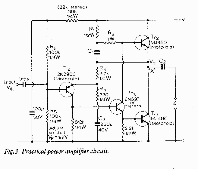 Gambar Skema Rangkain Audio Amplifier 10 Watt
This schematic is a 10 watt amplifier for audio frequencies (approx. 50Hz-20kHz). The circuit is extremely simple, comprised of a total of only 18 components, 4 of which are transistors. Of the transistors used, 1 is a PNP (2N3906) , and 3 are NPN (2n697, 2 x NJ480).
Source : www.electrokits.com
Source : www.electrokits.com
Kit Telephone Amplifier
Not a speakerphone, but a high performance isolated input amplifier that connects directly to a telephone line. Unlike a lot of amplifiers, this one provides both speaker output and line output. Speaker output is perfect for “group listen? applications with standard telephones for group gatherings without the inconvenience and interruption of vox operated speakerphones.
 |
| Kit Telephone Amplifier |
The K4900 also features line level output designed to be connected to the aux input of any standard audio mixer or amplifier. This makes it perfect for radio stations, home broadcasters, and larger applications that need to connect their phone line into their systems. Features a standard isolation transformer input for zero loading of the phone line. Speaker output is a half watt into 8 ohms. Line output is 0dB (.775Vrms). The circuit runs on 7-10VAC or 9-12VDC at 150mA.
Read MoreType and function of subwoofer speaker box
Know Your Types of box type subwoofer
 Following this, the types of subwoofer box that is often applied in car audio:
Read More..
Performance subwoofer to produce low bass sound and also solid course supported by a subwoofer enclosure or box. Subwoofer box in the car usually has a different size, it is adjusted to the recommendations of the technical data from these subwoofers. However, each audio installer, have different styles in a box design.
If all this time, we only know when the box was just the type thats all, it did not. Box consists of various types and models. Models, size (dimensions) and a subwoofer box models are usually clearly taken into account at the time of manufacture, even carefully designed too often acted the Installer. Clearly, each type of box has a value of strengths and weaknesses, all models of boxes, if applied correctly, clearly gives a very maximum performance subwoofer.
If you want us to categorize the type of subwoofer box can be divided according to several orders of more detail:
• Second Order / Infinite Baffle / Free Air
• Typical Rear Deck Installation / Infinite Baffle / Free
• Back Seat Installation
• Small Deck Installation
• Second Order / Acoustic Suspension / Sealed enclosures
• Sealed
• isobaric - Sealed
• isobaric - Sealed (Compound Loading)
• isobaric - Sealed (Back to Back)
• isobaric - Sealed (Planar Loading)
• Fourth Order / Bass Reflex & bandpass enclosures
• Fourth Order / Bass Reflex
• isobaric - Bass Reflex
• isobaric - Bass Reflex (Compound Loading)
• Bass Reflex - Passive Radiator
• isobaric Bass Reflex - Passive Radiator
• Single Reflex - Band Pass
• Single Reflex isobaric bandpass
• Three Chamber Single Reflex bandpass
• Three Chamber Single Reflex isobaric bandpass
• Sixth Order enclosures
• Quasi Sixth Order Series-Tuned bandpass
• isobaric Quasi Sixth Order Series-Tuned bandpass
• Dual reflex bandpass
• Dual Reflex isobaric bandpass
• Three Chamber Dual Reflex bandpass
• Three Chamber Dual Reflex isobaric bandpass
• Eighth Order enclosures
• Quasi Eighth Order Series-Tuned Dual Reflex bandpass
• Quasi isobaric Eighth Order Series-Tuned Dual Reflex bandpass
• Eighth Order Triple Reflex bandpass
• Eighth Order Triple Reflex isobaric bandpass
TDA7496 Low Noise Power Amplifier
Audio amplifier circuit given away now is a 5W stereo grade AB power amplifier based on the TDA7496 IC designed in favor of high-level quality sound.
 |
| TDA7496 Low Noise Power Amplifier |
The power supply required obligation cede 22 volts for 8 ohms load impedance and 12 volts for 4 ohms load impedance . The highest output power which can be located obtained with this audio IC is around 5.5 watts on 8 ohms load with 10 % THD and 4 watts with 1 % THD.
focal skin of the TDA7496 include linear volume control ,standpoint-by and Mute functions , 2 x 5Watt output power, undersized circuit protection , thermal overload protection.
- greatest extent ratings of TDA7496 IC
- Supply Voltage: 35 against
- Maximum Input Voltage: 8 Vpp
- full Power Dissipation (Tamb = 80°C): 15 W
- Operating fever: 0 to 70 °C
- cargo space and Junction fever: -40 to 150 °C
- Volume CTRL DC voltage: 7 vs.
Tuesday, December 24, 2013
230 400 Watt Power Amplifier MOSFET
Amplifier circuit below is a series of amplifiers with the amplifier transistor and mosfet. This amplifier output power ranging from 230W up to 400W.
 |
| 230 - 400 Watt Power Amplifier |
Wireless transmitter microphone circuit

Wireless FM transmitter circuit Microphone Hi Fi using a model-ready transmitters, this is because the buil-up transmitter module has a transmission capability of a stable and very effective to emit 10 mW RF. so that the target of Hi Fi FM Wireless Microphone transmitter circuit Hi Fi can be realized. The series can be seen from the FM transmitter Microphone Wireless Hi Fi transmitter module is that it stands alone with an additional R7, R8 and C6 to produce high-quality RF frequency.
In the series of FM transmitter Microphone Wireless Hi Fi module requires power consumption of a battery 12 VDC. Transmission antenna is directly connected with the circuit module Wireless FM transmitter Wireless FM Microphone Hi Fi.

Input section of the circuit transmitter Wireless FM Microphone Hi Fi signals to the modulation of 100mV RMS. A microphone preamplifier with IC TL081 is used to reproduce the signal from the microphone into a signal with 100mV rms level as needed this wireless FM transmitter module. strengthening the signal from the microphone preamplifier circuit in FM transmitter Microphone Wireless Hi Fiini regulated by P1. R1, R2 and C1 in the range of an FM transmitter Microphone Wireless Hi Fi is used to provide supply to the microphone electred used.
200W power amplifier complete power supply
This 200W power amplifier circuit using IC STK 4050.
STK 4050 is a power amplifier module is very powerful, because the IC is already a module then only needed a little extra components to build a reliable 200W Power Amplifier. Here is a picture series of Power Amplifier ICs 200W use STK 4050 complete with its power supply:
STK 4050 is a power amplifier module is very powerful, because the IC is already a module then only needed a little extra components to build a reliable 200W Power Amplifier. Here is a picture series of Power Amplifier ICs 200W use STK 4050 complete with its power supply:

Treatment LCD monitor
Treatment LCD Monitor. At this time computer use familiar and already widely used either for work or entertainment. And of course when talking about computers it will not be far away with a device called a monitor. And today use CRT monitors have started to decrease with the LCD Monitor that despite having a price that is quite expensive but have many advantages than conventional CRT monitors.
Here are a few advantages of LCD monitor is a stylish design, flat screen and a brighter color than convex or crt monitor screen, while also LCD Monitors have many advantages among which have a high resolution so that it can help many people especially those working Visual design field.
There are some special treatment for LCD monitors in this case is for the treatment of LCD monitors, the following are some steps steps:
Use the LCD as needed, Do not use if you do not need so-necessary and do not use it 24 hours nonstop jedanya have no time for any electronic item there during his lifetime (Lifetime). Turn off your LCD monitor when your computer dies, in order to save electricity and also keeps your LCD monitor remain durable.
Use the type that has a grounding electrical power, because it can minimize the damage in the event of lightning strikes. This option is optional.
Perform regular cleaning, at least 2 weeks 1 times, for LCD monitors are always in a state clear of dust and other debris. Remember! to clean it must use a very soft cloth that has spread with a special liquid cleaners LCD monitor. If necessary you can buy special equipment to clean the LCD monitor.
Do not engage in cleanup activities in the state of electricity is still flowing, unplug all cables available on the LCD to avoid things that are not desired. The existence of water coming into the series of LCD monitors will be able to cause fatal damage.
Keep the LCD of the things that contain water such as rain water, drinking water etc.. Because all electronic goods electrical short circuit will occur if water enters into the electronic components.
Keep the LCD of goods containing such magnetic sound system, Persani, HP etc. signals. Because it will be fatal is going to happen Noise or damage which may destroy the layout on the monitor screen.
LCD Save a strategic place and safe from the reach of small children, so that you can not avoid tersenggol LCD or a small toy.
Unplug all cables associated with the computer (including LCD) in the event of rain accompanied by lightning, because lightning can be grabbed via the antenna propagate through the cable TV and electricity.
To protect the screen / LCD screen can use the Screen Protector function prevents dust entry into the LCD and also take care of all sorts of scrapes. Remember to choose the screen protector is not a trace when reopened.
If there is damage to your LCD monitors, LCD submit to the experts. Do not disassemble itself without accompanied by experts in the field of electronics. Module Components including LCD monitors that can be easily damaged. LCD Monitor Service you to the service center to ensure the improvement is good and right.
Good article on the LCD monitor is beneficial treatment.
Monday, December 23, 2013
Crossover types
Crossover is a tool that serves to limit the "frequency range" to be received by the speaker. Crossover is used to regulate flow to the tweeter, the midrange, midwoofer, and bass to the subwoofer. There are two kinds of crossover, the crossover passive and active crossover.
 |
| passive crossover |
Passive crossovers work after receiving the output of the amplifier, are ineffective because they are throwing power amplifier, because the passive crossover frequencies have been processed in the "boost" (increase) by the amplifier.
 |
| active crossover |
Active crossovers work so signal generated by the head unit (pure signal), dividing it in accordance with the desired frequency boost later in the amplifier, so that the amplifier to work more efficiently, and frequencies produced more organized in accordance with their respective purposes, tweeter, midrange, woofer , subwoofer.
A little short in the use of an active crossover is the use of 12V power, ground, and remote. In theory this could lead to "noise" on the audio system, but do not worry, by the proper installation, and use good quality products will not occur a problem, as in any "competition-level car audio system". If you want to raise just a little audio sound quality, passive crossover is the right choice. But if want the sound quality is really good you should select an active crossover. Active crossovers require special mounting, especially for power cables and ground wires, but the effort is proportional to the quality of music produced. Active Crossover works by "cutting" is not frequency necessary before the "boost" by the amplifier, so the amplifier can focus on the frequency you want to hear, so do not waste energy Power.
Open Garage Door Using A Smartphone
You do almost anything with your mobile phone, but when it comes to your garage door, you have to resort to another remote control. This garage door opener does not require the installation of an application and it works with any phone that has a web browser built-in. The system is based on the tux-graphics Ethernet board. The circuit diagram has external connections, relay and optional connection to switch to sense the state of the door. The relay contacts are then to be connected in parallel to the wall mounted push buttons inside your garage. They mounted the Ethernet board on a small piece of wood together with some screw-on terminations for the cables.
 |
| Open Garage Door Using A Smartphone |
[source] Extremecircuit.net
2 Transistor Transmitter Schematic
A compact 2 transistor transmitter for use at VHF frequencies.
2 Transistor Transmitter Schematic Circuit Diagram

Notes:
Transistor T1 works as an audio preamplifier, gain is fixed at approximately R2/R1 or 100 times. The audio input is applied at the points LF in (on the diagram). P1 works as gain control. After amplification this audio signal now modulates the transmitter built around T2. Frequency is tunable using the trimmer CT and L1 is made using 3 turns of 1mm copper wire wound on a 5mm slug. The modulated signal passes via C6 to the antenna. A dipole can be made using 2 lengths of 65cm copper pipe. A DC power supply in the range 3 to 16 volts is required.
2 Transistor Transmitter Schematic Circuit Diagram
Transistor T1 works as an audio preamplifier, gain is fixed at approximately R2/R1 or 100 times. The audio input is applied at the points LF in (on the diagram). P1 works as gain control. After amplification this audio signal now modulates the transmitter built around T2. Frequency is tunable using the trimmer CT and L1 is made using 3 turns of 1mm copper wire wound on a 5mm slug. The modulated signal passes via C6 to the antenna. A dipole can be made using 2 lengths of 65cm copper pipe. A DC power supply in the range 3 to 16 volts is required.
Multiplexer with CMOS IC 4556
In addition to the family of TTL ICs that support the function of a multiplexer is a family of CMOS ICs.

Read More..
Despite the fact it is the family of TTL ICs that support more functions than the CMOS multiplexer. For the working principle of the multiplexer IC CMOS family is actually tantamount to a multiplexer circuit, or IC TTL logic gates. That should be all referring to the real multiplexer function, namely the determination of output lines which represent the number of input lines. The use of symbols is possible between TTL and CMOS IC has a different but actually run the same rules. For your reference if you are interested in using family of CMOS IC 4556 series in particular, I include also the truth table below:
INPUT | OUTPUT | |||||
E | A0 | A1 | O0 | O1 | O2 | O3 |
L | L | L | L | H | H | H |
L | H | L | H | L | H | H |
L | L | H | H | H | L | H |
L | H | H | H | H | H | L |
H | X | X | H | H | H | H |
L = LOW | ||||||
H = HIGH | ||||||
Sunday, December 22, 2013
Audio Amplifier Circuits 10W with Bass boost
 Parts:
P1 22K Log.Potentiometer (Dual-gang for stereo)
P2 100K Log.Potentiometer (Dual-gang for stereo)
R1 820R 1/4W Resistor
R2,R4,R8 4K7 1/4W Resistors
R3 500R 1/2W Trimmer Cermet
R5 82K 1/4W Resistor
R6,R7 47K 1/4W Resistors
R9 10R 1/2W Resistor
R10 R22 4W Resistor (wirewound)
C1,C8 470nF 63V Polyester Capacitor
C2,C5 100uF 25V Electrolytic Capacitors
C3,C4 470uF 25V Electrolytic Capacitors
C6 47pF 63V Ceramic or Polystyrene Capacitor
C7 10nF 63V Polyester Capacitor
C9 100nF 63V Polyester Capacitor
D1 1N4148 75V 150mA Diode
IC1 NE5532 Low noise Dual Op-amp
Q1 BC547B 45V 100mA NPN Transistor
Q2 BC557B 45V 100mA PNP Transistor
Q3 TIP42A 60V 6A PNP Transistor
Q4 TIP41A 60V 6A NPN Transistor
J1 RCA audio input socket
Power supply parts:
R11 1K5 1/4W Resistor
C10,C11 4700uF 25V Electrolytic Capacitors
D2 100V 4A Diode bridge
D3 5mm. Red LED
T1 220V Primary, 12 + 12V Secondary 24-30VA Mains transformer
PL1 Male Mains plug
SW1 SPST Mains switch
Comments:
This design is based on the 18 Watt Audio Amplifier, and was developed mainly to satisfy the requests of correspondents unable to locate the TLE2141C chip. It uses the widespread NE5532 Dual IC but, obviously, its power output will be comprised in the 9.5 - 11.5W range, as the supply rails cannot exceed ±18V.
As amplifiers of this kind are frequently used to drive small loudspeaker cabinets, the bass frequency range is rather sacrificed. Therefore a bass-boost control was inserted in the feedback loop of the amplifier, in order to overcome this problem without quality losses. The bass lift curve can reach a maximum of +16.4dB @ 50Hz. In any case, even when the bass control is rotated fully counterclockwise, the amplifier frequency response shows a gentle raising curve: +0.8dB @ 400Hz, +4.7dB @ 100Hz and +6dB @ 50Hz (referred to 1KHz).
Notes:Can be directly connected to CD players, tuners and tape recorders.
Schematic shows left channel only, but C3, C4, IC1 and the power supply are common to both channels.
Numbers in parentheses show IC1 right channel pin connections.
A log type for P2 ensures a more linear regulation of bass-boost.Dont exceed 18 + 18V supply.
Q3 and Q4 must be mounted on heatsink.
D1 must be in thermal contact with Q1.
Quiescent current (best measured with an Avo-meter in series with Q3 Emitter) is not critical.
Set the volume control to the minimum and R3 to its minimum resistance.
Power-on the circuit and adjust R3 to read a current drawing of about 20 to 25mA.Wait about 15 minutes, watch if the current is varying and readjust if necessary.
A correct grounding is very important to eliminate hum and ground loops. Connect in the same point the ground sides of J1, P1, C2, C3 &C4. Connect C9 at the output ground.
Then connect separately the input and output grounds at the power supply ground.
Technical data:
Output power: 10 Watt RMS @ 8 Ohm (1KHz sinewave)
Sensitivity: 115 to 180mV input for 10W output (depending on P2 control position)
Frequency response: See Comments above
Total harmonic distortion @ 1KHz: 0.1W 0.009% 1W 0.004% 10W 0.005%
Total harmonic distortion @ 100Hz: 0.1W 0.009% 1W 0.007% 10W 0.012%
Total harmonic distortion @10KHz: 0.1W 0.056% 1W 0.01% 10W 0.018%
Total harmonic distortion @ 100Hz and full boost: 1W 0.015% 10W 0.03%
Max. bass-boost referred to 1KHz: 400Hz = +5dB; 200Hz = +7.3dB; 100Hz = +12dB; 50Hz = +16.4dB; 30Hz = +13.3dB
Combine stereo input to one output
Here , I will give a circuit of schemes that are used to combine 2 pieces input or stereo to 1 input mono. Why 2 inputs in to one because, if we need a stereo amplifier we want to become a stronger by combining the two input into one input, so that a higher power output. Actually without any circuit above we can combine stereo amplifier into mono, but the sound output less than the maximum , need for this additional combiner circuit.

R1______150K
R2______920R
R3______150K
R4______920R
R5______920R
U1______NE5532
For balance _: R1 / R2=R3 / R4
For balance _: R1 = R3
Gain ______: R5 / R1 = R5 / R3
Simple Doubler Voltage 12 to 24Volt DC
This take place simple Doubler Voltage circuit, from voltage 12VDC to be 24VDC. By benefit Timer IC highly prevalent the come to NE555 and other equipment a modest again. It can make happen current contract in relation to 50mA fitting pro the circuit, with the intention of use low current the insignificant-sized.
 |
| Simple Doubler Voltage 12 to 24 VDC Schematic Diagram |
The belief facility of the circuit be present, at what time use Volt input 12VDC give with the circuit long for converge Filter current smoothly with increasingly. The capacitors C5 give with IC1, The resistor R1,R2 and , capacitors C1, Which build the circuit ideal astable multi vibrator open place wave generator, by the side of the frequency with reference to 2KHz befall shown the way pin 3 of IC1. By take capacitors C3,C4 diode D1 and D2. Which build come to pass boost up voltage x 2,which self-control enhance the level Volt out be the sincere current about 24VDC or else 2 time of the level Volt input.
Microphone Amplifier using MAT02
This microphone amplifier circuit electronic project is designed using MAT02 dual monolithic transistor and few passive electronic components .This microphone amplifier circuit allow use of microphones with different impedance and provides a voltage gain of 20 dB and 23.5 dB (amplification 10 and 15), selectable from a switch. Preamplifier has two stages with direct coupling and reaction, and the input stage operates at very low collector current to minimize the noise.

Output impedance is approximately 70 ohms at a gain of 23.5 dB. Low power consumption (approx. 2.5 mA) and power from a 9V battery make it ideal for portable applications. Since the resistor R3 is responsible for input impedance and a few other important features of preamplifier, with R3 = 220 k, the input impedance is 30 k. Change the value of R3 to 6.8 k input impedance dropped to about 1 k.
Saturday, December 21, 2013
TSC230 Color Sensor

Color Sensor TCS230 color sensor is a chip that works with the converting acceptance of a certain color of light emitted into the shape of frequency. TCS230 Color Sensor composed dri two main parts, namely a light-receiving section arranged in an array photodioda and Chaya koncerter this part to the frequency.
Basically the TCS230 Color Sensor is a light sensor which is equipped with light filters for RGB primary color (Red-Green-Blue) and light sensor without the filter with scale 8 bits for each of this part of the sensor.
Basically the TCS230 Color Sensor is a light sensor which is equipped with light filters for RGB primary color (Red-Green-Blue) and light sensor without the filter with scale 8 bits for each of this part of the sensor.
Photodiode the TCS230 Color Sensor arrays arranged in 8 × 8 with the internal configuration of the photodiode. 16 photodiode for the light sensor with a red light filter. 16 photodiode for the light sensor with a green light filter. 16 photodiode for the light sensor with a blue light filter. And 16 photodiode for light sensor without a color filter. On the use of Color Sensor TCS230 we can choose the color sensor with a filter of what we want to set the configuration data S2 and S3.
 |
| Pin-Out TSC230 |
Photodiode the TCS230 Color Sensor will issue a magnitude comparable with current levels of primary color of light that happened to him. This current is then converted into pulses with a frequency proportional to the amount of current. TCS230 Color Sensor Output frequency can be made by adjusting the scale of the configuration data S0 and S1 of the selector pins S0 and S1 Color Sensor TCS230.
Adjustable switching power supply
 |
Switching Regulator L4970 series include not complicated to make his own, which need to be considered is the IC L4970 require sufficient cooling to operate in an optimal and durable. Adjustable Switching Regulator L4970 series are complete can be seen in thethe following figure .
 |
| Adjustable switching power supply schematics |
To set the output voltage range Adjustable Switching Regulator L4970 can be in control by adjusting the potentiometer 18KOhm tus.
TDA2006 12W Audio Amplifier Circuit
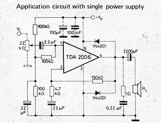 This 12w amplifier circuit is build round the TDA2006 integrated circuit who options a brief circuit protection system, and a thermal shutdown system in case of overheating. With a 12v power supply the circuit delivers 12w on a 4 ohm speaker and 8w on a 8 ohm speaker. The integrated circuit will work with a power supplyr between 6v and 15v max.
The TDA2006 is monolithic integrated circuit in package, {supposed to be used as a low frequency category "AB" amplifier. At ±12V, d = 10 and frequently it provides 12W output power on a 4Ω load and 8W on a 8Ω . The TDA2006 provides high output current and has terribly low harmonic and cross-over distortion. any the device incorporates an inspired (and patented) short circuit protection system comprising a rendezvous for automatically limiting the dissipated power therefore on keep the operating urpose of the output transistors at intervals their safe operating space. a standard thermal shutdown system is additionally included. The TDA2006 is pin to pin equivalent to the TDA2030
Regulated 24 Watt Broad Spectrum LED Lamp
This project involves constructing an energy efficient broad spectrum LED lamp system. The lamp is useful for indoor reflective room lighting. It has a broad color spectrum that more closely approximates the light of the sun when compared to fluorescent bulbs and white-only LEDs. The light level is regulated and the light that is produced does not flicker. The six differently colored LED stars, made by LedEngin, Inc., are rated at 5 watts (nominal). The LED array and associated current regulator consume 1 amp at 24VDC (24 Watts). NEVER stare directly at this lamp when it is running at full operating power, it is DANGEROUSLY BRIGHT.

With the LEDs shown, the combined color of the lamp has a pinkish white hue. The 5 Watt ratings of the LEDs are not precise, the white, blue and green LEDs consume about 4W and the lower voltage red, orange and deep red LEDs consume about 3W. The current regulator keeps the LED brightness constant and insures that the LED series string never draws more than 1 amp of current.
The project has also been coined "Bold as LED" in reference to the Jimi Hendrix song "Bold as Love" which has the lyric: "My yellow in this case is not so mellow".
Specs:
The lamp is wired as a current loop which includes the power supply, the LED series string and the 1 amp current regulator circuit. The LM317K and 1.2 ohm 5 Watt resistor act as a current regulator that limits the loop current to 1 Amp. During regulation, there will always be 1.2V across the 1.2 ohm resistor. The current regulator insures that the LEDs always run at their maximum brightness, but not so bright that they burn out. A 100uF electrolytic capacitor bypasses the DC power input to the device and a 100nF monoblock capacitor bypasses the LM317K input.
Construction:
The LEDs and current regulator circuit were mounted on a 3" x 8" chunk of 1/8" aluminum stock. The LM317K regulator and LED heat sinks were bolted to the chassis directly, heat sink grease was used on the regulator, the heat sinks and the six LEDs. Connecting the LM317K directly to the aluminum plate makes the plate electrically hot at 1.2V, the plate should not be allowed to come into contact with any live conductors. By using a few more parts, the LM317 can be mounted with an insulator and plastic shoulder washers for electrical isolation from the mounting plate.
The LEDs come mounted on their own small star-shaped aluminum substrates, these were attached to the aluminum plate using two 7/16" 4-40 screws and nuts per LED. A drop of silicone heat sink grease should be applied to the center of each LED star when it is mounted to the plate for heat conduction. It is important to use insulating plastic washers on the top side of the LED stars to prevent electrical contact with head of the screw. The LED stars were soldered together using short pieces of #20 tinned wire after being mounted on the plate. It is necessary to use a fair amount of heat to solder the contacts, a 200/240W soldering gun did the job. Be very careful not to melt the lenses on the LEDs, the LEDs cost around $10 each. The positive and negative leads of the LED series string were connected back to the current reglator circuitry using #20 wire covered with teflon insulation.
The initial mechanical arrangement did not pass the "rule of thumb" test, which says that if a semiconductor is too hot to hold your thumb on, it will not live a long life. Two large aluminum heat sinks were bolted to the back of the aluminum plate and seem to be sufficient to keep the lamp operating at a reasonable temperature. The LED array produces more heat than the LM317K.
Use:
Connect this circuit to a 24VDC power supply or other power source such as a solar-charged lead acid battery. Be sure to observe the correct polarity. Look away from the LEDs and apply power. Again, do not stare directly at the LEDs, they are bright enough to harm your vision. A switch-mode power supply rated at 24VDC and 1 Amp or more is probably the most energy-efficient way to power this device from line power.
Parts:
1x LM317K T03 case 1.5A adjustable voltage regulator
1x 1.2 ohm 5W resistor (or 2x 2.4 ohm 2W resistors in parallel)
1x 100uF 35V or higher electrolytic capacitor
1x 100nF 35V or higher monolythic capacitor
1x LedEngin LZ1-10R205 deep red 5W LED
1x LedEngin LZ1-10R105 red 5W LED
1x LedEngin LZ1-10A105 amber 5W LED
1x LedEngin LZ1-10G105 green 5W LED
1x LedEngin LZ1-10B105 blue 5W LED
1x LedEngin LZ1-10CW05 cool white 5W LED
Miscellaneous wire, solder lugs, termination strips and hardware,
Large aluminum mounting plate, heat sinks if necessary.
With the LEDs shown, the combined color of the lamp has a pinkish white hue. The 5 Watt ratings of the LEDs are not precise, the white, blue and green LEDs consume about 4W and the lower voltage red, orange and deep red LEDs consume about 3W. The current regulator keeps the LED brightness constant and insures that the LED series string never draws more than 1 amp of current.
The project has also been coined "Bold as LED" in reference to the Jimi Hendrix song "Bold as Love" which has the lyric: "My yellow in this case is not so mellow".
Specs:
- Nominal operating power: 24 Watts (24V DC at 1 Amp)
- LED power consumption above regulation point: 18.6 Watts
- Maximum operating voltage: 28V DC
- Minimum voltage for regulated light: 23V DC
- Leds produce light down to 11V
- Deep Red LED voltage: 2.55V
- Red LED voltage: 2.37V
- Amber LED voltage: 2.60V
- Green LED voltage: 3.92V
- Blue LED voltage: 3.56V
- White LED voltage: 3.7V
- Voltage across regulator when current becomes regulated: 4.2V
The lamp is wired as a current loop which includes the power supply, the LED series string and the 1 amp current regulator circuit. The LM317K and 1.2 ohm 5 Watt resistor act as a current regulator that limits the loop current to 1 Amp. During regulation, there will always be 1.2V across the 1.2 ohm resistor. The current regulator insures that the LEDs always run at their maximum brightness, but not so bright that they burn out. A 100uF electrolytic capacitor bypasses the DC power input to the device and a 100nF monoblock capacitor bypasses the LM317K input.
Construction:
The LEDs and current regulator circuit were mounted on a 3" x 8" chunk of 1/8" aluminum stock. The LM317K regulator and LED heat sinks were bolted to the chassis directly, heat sink grease was used on the regulator, the heat sinks and the six LEDs. Connecting the LM317K directly to the aluminum plate makes the plate electrically hot at 1.2V, the plate should not be allowed to come into contact with any live conductors. By using a few more parts, the LM317 can be mounted with an insulator and plastic shoulder washers for electrical isolation from the mounting plate.
The LEDs come mounted on their own small star-shaped aluminum substrates, these were attached to the aluminum plate using two 7/16" 4-40 screws and nuts per LED. A drop of silicone heat sink grease should be applied to the center of each LED star when it is mounted to the plate for heat conduction. It is important to use insulating plastic washers on the top side of the LED stars to prevent electrical contact with head of the screw. The LED stars were soldered together using short pieces of #20 tinned wire after being mounted on the plate. It is necessary to use a fair amount of heat to solder the contacts, a 200/240W soldering gun did the job. Be very careful not to melt the lenses on the LEDs, the LEDs cost around $10 each. The positive and negative leads of the LED series string were connected back to the current reglator circuitry using #20 wire covered with teflon insulation.
The initial mechanical arrangement did not pass the "rule of thumb" test, which says that if a semiconductor is too hot to hold your thumb on, it will not live a long life. Two large aluminum heat sinks were bolted to the back of the aluminum plate and seem to be sufficient to keep the lamp operating at a reasonable temperature. The LED array produces more heat than the LM317K.
Use:
Connect this circuit to a 24VDC power supply or other power source such as a solar-charged lead acid battery. Be sure to observe the correct polarity. Look away from the LEDs and apply power. Again, do not stare directly at the LEDs, they are bright enough to harm your vision. A switch-mode power supply rated at 24VDC and 1 Amp or more is probably the most energy-efficient way to power this device from line power.
Parts:
1x LM317K T03 case 1.5A adjustable voltage regulator
1x 1.2 ohm 5W resistor (or 2x 2.4 ohm 2W resistors in parallel)
1x 100uF 35V or higher electrolytic capacitor
1x 100nF 35V or higher monolythic capacitor
1x LedEngin LZ1-10R205 deep red 5W LED
1x LedEngin LZ1-10R105 red 5W LED
1x LedEngin LZ1-10A105 amber 5W LED
1x LedEngin LZ1-10G105 green 5W LED
1x LedEngin LZ1-10B105 blue 5W LED
1x LedEngin LZ1-10CW05 cool white 5W LED
Miscellaneous wire, solder lugs, termination strips and hardware,
Large aluminum mounting plate, heat sinks if necessary.
Friday, December 20, 2013
Dual Tracking regulator circuit
A IC MAX634 inverting regulator is combined with a IC MAX630 to provide a dual tracking approximately 15 Volt output from a 12 Volt DC battery. The reference for the - 15 Volt output is derived from the positive output via R3 and R4. Both regulators are set to maximize output power at low battery voltages by reducing the oscillator frequency , via LBR, when V Batt falls to 8,5 volt.
Technical instruction :
Max. Input voltage : 13 Volt / N/a mA
Max. Output voltage :-15 Volt , + 15 volt / 45 mA
Tracking FM Transmitter Schematics
FM tracer was prepared using the LM3909 IC and some supporting components. 1.5V FM trackers This will provide an indicator of revenue sources by providing a signal emitted by the LED. FM tracking uses a source voltage of the battery cell and fruit consumption current is 3.7 mA.
After completion of assembling Tracker FM 1.5V, then the next step is setting the operating frequency of the FM tracker is, for convenience we can use the FM receiver and adjust the working frequency FM 1.5V Tracking (tracking transmitter) by regulating C3.Have been obtained if the working frequency Tracking FM 1.5V (tracking transmitter) then the corresponding LED will light emitted by the transmitter information such as sound through an FM receiver is terdengan. 1.5V FM tracker (tracking transmitter) can use a regular 12-inch antenna. Playing and learning electronics that will be happy,
1.5 Volt Tracking FM circuit (Tracking Transmitter)
Circuit Description 1.5 Volt Tracking FM (Tracking Transmitter)
- For stability, use a NPO types for C2 & C4.
- Tolerance for R1 should be 1 or 2%.
- Frequency range is usually 87-109Mhz FM.
- Email wire used in wire coil is made of hookup 22 ga, like the solid Bell phone wire.
Subscribe to:
Posts (Atom)