Thursday, February 27, 2014

Flashing LED Battery status Indicator

Signals when an on-circuit battery is exhausted 5V to 12V operating voltage
A Battery-status Indicator circuit can be useful, mainly to monitor portable Test-gear instruments and similar devices. LED D1 flashes to attire the users attention, signaling that the circuit is running, so it will not be left on by mistake. The circuit generates about two LED flashes per second, but the mean current drawing will be about 200µA. Transistors Q1 and Q2 are wired as an uncommon complementary astable multivibrator: both are off 99% of the time, saturating only when the LED illuminates, thus contributing to keep very low current consumption. 

Circuit diagram :
Flashing-LED Battery
Flashing-LED Battery-status Indicator Circuit Diagram

The circuit will work with battery supply voltages in the 5 - 12V range and the LED flashing can be stopped at the desired battery voltage (comprised in the 4.8 - 9V value) by adjusting Trimmer R4. This range can be modified by changing R3 and/or R4 value slightly.

When the battery voltage approaches the exhausting value, the LED flashing frequency will fall suddenly to alert the user. Obviously, when the battery voltage has fallen below this value, the LED will remain permanently off. To keep stable the exhausting voltage value, diode D1 was added to compensate Q1 Base-Emitter junction changes in temperature. The use of a Schottky-barrier device (e.g. BAT46, 1N5819 and the like) for D1 is mandatory: the circuit will not work if a common silicon diode like the 1N4148 is used in its place.

Parts :
R1,R7__________220R  1/4W Resistors
R2_____________120K  1/4W Resistor
R3_______________5K6 1/4W Resistor
R4_______________5K  1/2W Trimmer Cermet or Carbon
R5______________33K  1/4W Resistor
R6_____________680K  1/4W Resistor
R8_____________100K  1/4W Resistor
R9_____________180R  1/4W Resistor
C1,C2____________4µ7  25V Electrolytic Capacitors
D1____________BAT46  100V 150mA Schottky-barrier Diode
D2______________LED  Red 5mm.
Q1____________BC547   45V 100mA NPN Transistor
Q2____________BC557   45V 100mA PNP Transistor
B1_______________5V to 12V Battery supply
Notes :
  • Mean current drawing of the circuit can be reduced further on by raising R1, R7 and R9 values.
Source : Red Circuits
Read More..

Electronic Circuits for the Evil Genius 2nd Edition 64 Lessons

WE CASUALLY ACCEPT ELECTRONICS in our everyday world. Those who don’t understand how it works are casually obedient. Those who take the time to learn electronics are viewed as geniuses. Do you want to learn how to control the power of electronics? This text provides a solid introduction to the field of electronics, both analog and digital. Electronic Circuits for the Evil Genius is based on practical projects that exercise the genius that exists in all of us. Download ebook for full details and articles.

File Type: PDF
File Size:15MB
Total Pages: 321

PART ONE Components
  1. Components
  2. Resist If You Must
  3. More Components and Semiconductors
  4. Two Projects and Then Some More
PART TWO Introduction to Digital Electronics
  1. Digital Logic
  2. The First NAND Gate Circuit
  3. Analog Switches for Digital Circuits
  4. The NAND Gate Oscillator
  5. How Do We Understand What We Can’t See? .
  6. Digital Logic Project
PART THREE Counting Systems in Electronics
  1. Introducing an Analog-to-Digital Converter
  2. The 4017 Walking Ring Counter
  3. Running a Seven-Segment Display
  4. Define, Models, and Make Your Own Project
PART FOUR Amplifiers: What They Are and How to Use Them
  1. What Is an Amplifier?
  2. Exploring the Op Amp
  3. Applying the Op Amp: Building the Intercom
  4. Prototype and Models: Patience Has Its Rewards
PART FIVE Appendices
  • Common Component Packaging
  • Capacitors: Reading and Decoding
  • Animations List
  • Glossary.
  • Make Your Own Printed Circuit Boards
Read More..

Remote Audio Level Indicator

The normal level-indicator circuits which are available in the market require connections to be made to the output of the player, which may not be easily accessible. The audio level indicator circuit described here removes this restriction as it may be placed close to the player’s speakers and yet the desired effect can be realised. 

Circuit diagram :
Remote Audio Level Indicator-Circuit Diagram
Remote Audio Level Indicator Circuit Diagram

As shown in the circuit, signals are picked up by the condenser microphone, which get further amplified by the noninverting amplifier built around one of the four op-amps of LM324. The remaining three, along with four op-amps of the second LM324, are used as seven comparators to work as the level detector, giving seven output levels through seven coloured LEDs. 

The sensitivity of the audio level indicator circuit may be improved by varying the 220k potentiometer. If a fine adjustment is desired, a 4.7-kilohm potentiometer may be connected in series resistors with the 220k potentiometer.


Copyright : EFY
Read More..

Basic IC MonoStable Multivibrator


Basic LM555 Timer CIRCUIT

Part List
C2 = .01uf
IC1 = LM555 Timer
SWI = n.o. momentary switch
R1 and C1 determine lenght of
out put pulse where  t = R1 x C1
and R1 is in ohms and C1 is in farads .

by Tony van Roon
Read More..

Target 3001 V13 PCB POOL Edition

TARGET 3001! is a CAD-/CAE-software for PCB design. The integration of the schematic-, simulation- and layout data into one user interface, and the integration of these data into one file is revolutionary to the work of the design engineer. The aim is a short time-to-market of your products abandoning internal conversion struggles.

The TARGET 3001! Wiki intends to give information on TARGET 3001! It assists you to get started immediately. It shows you how to deal with common tasks, gives you helpful information and points at new important features.

TARGET 3001! itself consists of schematic, mixed mode simulation, contour autorouter, autoplacer, PCB layout, 3D view, basic EMC check, front panel layout. It provides manufacturing data for production processes of all industry standards.


Screenshoot:

  Broken Charger-Connection Indicator Circuit Schematic Diagram


Author:
Ing.-Büro FRIEDRICH
Website:
http://www.pcb-pool.com/
License:
Freeware
Read More..

Cheapest Ever Motion Sensor

The RS-455-3671 sensor used in the Automatic Rear Bicycle Light project published in  the July/August 2010 edition can be replaced by a motion sensor that costs nothing instead of a fiver or thereabouts. 

Cheapest Ever Motion Sensor-image 
The replacement is a homemade device, built from components easily found in the workshop of any electronics enthusiast. Effectively it works as a variable resistor, depending on the acceleration force to which the device is  submitted. A prototype presented a resistance of 200 kΩ when not moving, and 190 kΩ when dropping about 1 cm.
Cheapest Ever Motion Sensor-Circuit diagram
Constructing is easy. Cut off a piece of about 10 mm of copper tubing. Take a piece of conductive foam, the kind used to protect integrated circuits. Cut a rectangular piece of 10  x 50 mm. Roll up firmly until it can be push-fitted securely into the copper cylinder. Then insert a conductive wire through the centre of the cylinder, bend it and (optionally) add protective plastic sleeving to each side. This is the first contact. Finally, solder a thin wire to the copper cylinder. This is the second contact. The foam resistance is pressure dependent. 

Consequently, when the device moves due to an external force, the inertia of the cylinder causes varying pressure in the foam, resulting in a small change of resistance between the inner conductor and  the cylinder. Because of that, it’s important to ensure the cylinder vibration is not restricted in any way by the connecting wire or the PCB. 

The comparator circuit shown here is capable of resolving the resistance change of the proposed foam/wire/copper sensor, allowing it to detect the motion of a vehicle for alarm or other purposes. 


Author : Antoni Gendrau – Copyright : Elektor
Read More..

Wednesday, February 26, 2014

Mains Slave Switcher

There are many situations where two or more pieces of equipment are used together and to avoid having to switch each item on separately or risk the possibility of leaving one of them on when switching the rest off, a slave switch is often used. Applications which spring to mind are a computer/printer/scanner etc or audio amplifier/record deck/tuner combinations or perhaps closest to every electronics enthusiast’s heart, the work bench where a bench power supply/oscilloscope/soldering iron etc are often required simultaneously.

The last is perhaps a particularly good example as the soldering iron, often having no power indicator, is invariably left on after all the other items have been switched off. Obviously the simplest solution is to plug all of the items into one extension socket and switch this on and off at the mains socket but this is not always very convenient as the switch may be difficult to reach often being behind or under the work bench. Slave switches normally sense the current drawn from the mains supply when the master unit is switched on by detecting the resulting voltage across a series resistor and switching on a relay to power the slave unit(s).
mains-slave-switcher-circuit diagrams

This means that the Live or Neutral feed must be broken to allow the resistor to be inserted. This circuit, which is intended for switching power to a work bench when the bench light is switched on, avoids resistors or any modifications to the lamp or slave appliances by sensing the electric field around the lamp cable when this is switched on. The lamp then also functions as a ‘power on’ indicator (albeit a very large one that cannot be ignored) that shows when all of the equipment on the bench is switched on.

The field, which appears around the lamp cable when the mains is connected, can be sensed by a short piece of insulated wire simply wrapped around it and this is amplified by the three stage amplifier which can be regarded as a single super-transistor with a very high gain. The extremely small a.c. base current results in an appreciable collector current which after smoothing (by C3) is used to switch on a relay to power the other sockets. Power for the relay is obtained from a capacitor ‘mains dropper’ that generates no heat and provides a d.c. supply of around 15 volts when the relay is off.

Circuit diagram:
mains-slave-switcher-circuit-diagram
Mains Slave Switcher Circuit Diagram

The output current of this supply is limited so that the voltage drops substantially when the relay pulls in but since relays require more current to operate them than they do to remain energized, this is not a problem. Since the transistor emitter is referenced to mains Neutral, it is the field around the mains Live which will be detected. Consequently, for correct operation the Live wire to the lamp must be switched and this will no doubt be the case in all lamps where the switch is factory fitted. In case of uncertainty, a double-pole switch to interrupt both the Live and Neutral should be used.

The sensitivity of the circuit can be increased or decreased as required by altering the value of the T2 emitter resistor. The sensing wire must of course be wrapped around a section of the lamp lead after the switch otherwise the relay will remain energized even when the lamp has been switched off. The drawing shows the general idea with the circuit built into the extension socket although, depending on the space available an auxiliary plastic box may need to be used.

Warning:
The circuit itself is not isolated from the mains supply so that great care should be taken in its construction and testing. The sensor wire must also be adequately insulated and the circuit enclosed in a box to make it inaccessible to fingers etc. when it is in use.


http://www.ecircuitslab.com
Read More..

Clipping Indicator For Audio Amplifiers

A clipping indicator is a useful accessory on any audio amplifier. It indicates when the amplifier has reached its limit and is clipping the peaks of the audio signal. In practice, quite a lot of clipping can occur before you can hear it. So why is it necessary to know when an amplifier is clipping if you cant notice it? The answer is that clipping "squares up" the waveform and square waves contain lots of higher-frequency harmonics which can easily damage the tweeters in loudspeaker systems. This circuit is a true clipping indicator as opposed to the level indicators that are commonly used in preamplifier stages.

The problem with level indicators is that an amplifiers maximum output power is not constant. Thats because the amplifiers supply rails are not regulated and so the maximum power available at any given instant varies, depending on the applied signal. The circuit is quite simple and is based on two BD140 PNP transistors and zener diode ZD1. During normal operation, Q1 is turned on via ZD1 and R1. As a result, Q2 is held off (since its base is pulled high) and so LED1 is also off. However, if the output signal subsequently rises to within 4.7V of the positive supply rail, Q1 turns off since it no longer has any forward bias on its base.

Circuit diagram:
clipping-indicator-for-audio amplifiers
Clipping Indicator Circuit Diagram

As a result Q2s base is now pulled low via R2 and so Q2 turns on and lights LED1. (Note: the 0.6V drop across Q1s base/emitter is ignored here because ZD1 conducts before its rated voltage due to the very low current involved). Why choose 4.7V below the power rail as the turn-on point? The reason is that, due to the drive limitations and the nature of emitter followers, they can be expected to have at least 4V across them when they saturate (ie, clip). ZD1 can be increased to a 5V or 6.2V type if the circuit is to be used with a monster amplifier.

The value of R3 should be customized according to the amplifiers supply rail, so that LED1 operates with the correct brightness. To do that, first measure the amplifiers positive supply voltage, then use Ohms Law (R = V/I) to calculate the value of R3 for a current of about 20mA. As it stands, this circuit can only be used to monitor the positive-going half-cycles of the audio waveform. If you want to monitor the negative half-cycles as well, you will have to build a second circuit with the following changes: (1) reverse both LED1 and ZD1; and (2) use BD139 (NPN) transistors for Q1 & Q2. Note that, in both cases, you should use the earth inside the amplifier, as the speaker negative may not be earth (such as in a bridged output).


Author: Philip Chugg - Copyright: Silicon Chip Electronics Magazine
Read More..

Speech Filter

In communications receivers and microphone amplifiers for transmitting equipment, there is frequently a need for a narrow, low-frequency band-pass filter that lets only the voice band through. This band is usually defined to be the portion of the audio frequency spectrum between approximately 300 Hz and 3300 Hz. In order to implement such a filter, we have calculated the values for two fifth-order Butterworth filters having these corner frequencies and connected them in series. The result is a band-pass filter for the desired pass-band with a skirt steepness of 100 dB/decade.  The first opamp (IC1) acts as a buffer.
Speech Filter Image :
image
The circuit can be powered by a unipolar supply voltage between 5 V and 18 V, which is a broad enough range that it should always be possible to find a suitable voltage when building the filter into existing equipment. The current consumption of the filter is only a few milliampères, which should rarely pose a problem. There is fairly wide selection of suitable candidates for the opamps, since the circuit is not critical in this regard. In addition to the indicated OP27A, you could consider using a TL081N or even an old-fashioned 741.
Circuit diagram : 
Speech-Filter-Circut-Diagram
Speech Filter Circuit Diagram
Due to unavoidable spreads in component values, the pass-band curve of the filter will never be completely perfect in actual practice. However, the deviations will be very small and in any case inaudible. In the pass-band region, the gain is approximately unity. The printed circuit board design shown here allows the speech filter to be built in a very compact form, which can be an important factor if it must be fitted into existing equipment. You can quickly check the fully assembled circuit by momentarily measuring the voltages at the inputs and out-puts of the three opamps. Half of the supply voltage should be present at all of these locations.
PCB Layout :
Pcb Lyout
Parts LIST:
Resistors:
R1.R2 = 22kΩ
R3,R11,R12,R18,R19 = 100kΩ
R4 = 470Ω
R5 = 150Ω
R6 = 10kΩ
R7 = 18kΩ
R8 = 15kΩ
R9 = 33kΩ
R10 = 82kΩ
R13-R17 = 3kΩ3
Capacitors:
C1,C8,C14,C15 = 100nF
C2 = 1µF MKT
C3-C7,C11 = 22nF
C9 = 33nF
C10 = 18nF
C12 = 10nF
C13 = 4nF7
C16,C17 = 10µF 16V
Semiconductors:
IC1,IC2,IC3 = OP27A, TL081CN
Miscellaneous:
Bt1 = 9-V battery
Author: G.Baars
Read More..

Mains Manager

Very often we forget to switch off the peripherals like monitor, scanner, and printer while switching off our PC. The problem is that there are separate power switches to turn the peripherals off. Normally, the peripherals are connected to a single of those four-way trailing sockets that are plugged into a single wall socket. If that socket is accessible, all the devices could be switched off from there and none of the equipment used will require any modification. 

Here is a mains manager circuit that allows you to turn all the equipment on or off by just operating the switch on any one of the devices; for example, when you switch off your PC, the monitor as well as other equipment will get powered down automatically. You may choose the main equipment to control other gadgets. 

The main equipment is to be directly plugged into the master socket, while all other equipment are to be connected via the slave socket. The mains supply from the wall socket is to be connected to the input of the mains manager circuit. The unit operates by sensing the current drawn by the control equipment/load from the master socket. On sensing that the control equipment is on, it powers up the other (slave) sockets.

The load on the master socket can be anywhere between 20 VA and 500 VA, while the load on the slave sockets can be 60 VA to 1200 VA. During the positive half cycle of the mains AC supply, diodes D4, D5, and D6 have a voltage drop of about 1.8 volts when current is drawn from the master socket. Diode D7 carries the current during negative half cycles. Capacitor C3, in series with diode D3, is connected across the diode combination of D4 through D6, in addition to diode D7 as well as resistor R10. Thus current pulses during positive half-cycles, charge up the capacitor to 1.8 volts via diode D3. 

This voltage is sufficient to hold transistor T2 in forward biased condition for about 200 ms even after the controlling load on the master socket is switched off. When transistor T2 is ‘on’, transistor T1 gets forward biased and is switched on. This, in turn, triggers Triac 1, which then powers the slave loads. Capacitor C4 and resistor R9 form a snubber network to ensure that the triac turns off cleanly with an inductive load.

Circuit diagram:
mains-manager circuit diagram
Mains Manager Circuit Diagram

LED1 indicates that the unit is operating. Capacitor C1 and zener ZD1 are effectively in series across the mains. The resulting 15V pulses across ZD1 are rectified by diode D2 and smoothened by capacitor C2 to provide the necessary DC supply for the circuit around transistors T1 and T2. Resistor R3 is used to limit the switching-on surge current, while resistor R1 serves as a bleeder for rapidly discharging capacitor C1 when the unit is unplugged. LED1 glows whenever the unit is plugged into the mains. Diode D1, in anti-parallel to LED1, carries the current during the opposite half cycles. Don’t plug anything into the master or slave sockets without testing the unit.

If possible, plug the unit into the mains via an earth leakage circuit breaker. The mains LED1 should glow and the slave LED2 should remain off. Now connect a table lamp to the master socket and switch it ‘on’. The lamp should operate as usual. The slave LED should turn ‘on’ whenever the lamp plugged into slave socket is switched on. Both lamps should be at full brightness without any flicker. If so, the unit is working correctly and can be put into use.

Note:
  1. The device connected to the master socket must have its power switch on the primary side of the internal transformer. Some electronic equipment have the power switch on the secondary side and hence these devices continue to draw a small current from the mains even when switched off. Thus such devices, if connected as the master, will not control the slave units correctly. 
     
  2. Though this unit removes the power from the equipment being controlled, it doesn’t provide isolation from the mains. So, before working inside any equipment connected to this unit, it must be unplugged from the socket.


http://www.ecircuitslab.com/2011/05/mains-manager.html
Read More..

Multitasking Pins Circuit

It’s entirely logical that low-cost miniature microcontrollers have fewer ‘legs’ than their bigger brothers and sisters – sometimes too few. The author has given some consideration to how to economise on pins, making them do the work of several. It occurred that one could exploit the high impedance feature of a tri-state output. In this way the signal produced by the high impedance state could be used for example as a CS signal of two ICs or else as a RD/ WR signal. 

Circuit diagram:
multitasking pins circuit diagram Multitasking Pins Circuit Diagram

All we need are two op-amps or comparators sharing a single operating voltage of 5 V and outputs capable of reaching full Low and High levels in 5-V operation (preferably types with rail-to-rail outputs). Suitable examples to use are the LM393 or LM311.The resistances in the voltage dividers in this circuit are uniformly 10 kilo ohms. Consequently input A lies at half the operating voltage (2.5 V), assuming nothing is connected to the input – or the microcontroller pin connected is at high impedance. 

The non-inverting input of IC1A lies at two thirds and the inverting input of IC1B at one third of the operating voltage, so that in both cases the outputs are set at High state. If the microcontroller pin at input A becomes Low, the output of IC1B becomes Low and that of IC1A goes High. If A is High, everything is reversed.
Read More..

Fuel Reserve Indicator For Vehicles

Here is a simple circuit for monitoring the fuel level in vehicles. It gives an audiovisual indication when the fuel level drops alarmingly below the reserve level, helping you to avoid running out of petrol on the way. Nowadays vehicles come with a dash-mounted fuel gauge meter that indicates the fuel levels on an analogue display. The ‘reserve’ level is indicated by a red marking in some vehicles, but the needle movement through the red marking may be confusing and not precise. This circuit monitors the fuel tank below the reserve level and warns through LED indicators and audible beeps when the danger level is approaching. 

Circuit diagram :
Fuel Reserve Indicator For Vehicles Circuit diagram
Fuel Reserve Indicator For Vehicles Circuit Diagram

The fuel sensor system consists of a tank-mounted float sensor and a current meter (fuel meter), which are connected in series. The float-driven sensor attached to an internal rheostat offers high resistance when the tank is empty. When the tank is full, the resistance decreases, allowing more current to pass through the meter to give a higher reading. The fuel monitoring circuit works by sensing the voltage variation developed across the meter and activates the beeper when the fuel tank is almost empty. Its point A is connected to the input terminal of the fuel meter and point B is connected to the body of the vehicle. The circuit consists of an op-amp IC CA3140 (IC1), two 555 timer ICs (IC2 and IC3) and decade counter CD4017 (IC4). 

Op-amp IC CA3140 is wired as a voltage comparator. Its inverting input (pin 2) receives a reference voltage controlled through VR1. The non-inverting input (pin 3) receives a variable voltage tapped from the input terminal of the fuel meter through resistor R1. When the voltage at pin 3 is higher han at pin 2, the output of IC1 goes high and the green LED (LED1) glows. This condition is maintained until the voltage at pin 3 drops below that at pin 2. When this happens, the output of IC1 swings from high to low, sending a low pulse to the trigger pin of the monostable (usually held high by R3) via C1. The monostable triggers and its output goes high for a predetermined time based on the values of R5 and C2. With the given values, the ‘on’ time will be around four minutes. 

The output of IC2 is used to power the astable circuit consisting of timer 555 (IC3) via diode D2. Oscillations of IC3 are controlled by R6, R7, VR2 and C4. With the given values, the ‘on’ and ‘off’ time periods are 27 and 18 seconds, respectively. The pulses from IC3 are given to the clock input (pin 14) of decade counter CD4017 (IC4) and its outputs go high one by one. When the circuit is switched on, LED1 and LED2 glow if your vehicle has sufficient petrol in the tank. 

When the fuel goes below the reserve level, the output of IC1 goes low, LED1 turns off and a negative triggering pulse is received at pin 2 of IC2. The output of IC2 goes high for around four minutes and during this time period, clock pin 14 of IC4 receives the clock pulse (low to high) from the output of IC3. For the first clock pulse, Q0 output of IC4 goes high and the green LED (LED2) glows for around 50 seconds. On receiving the second clock pulse, Q1 goes high to light up the yellow LED (LED3) and sound the buzzer for around 45 seconds. This audio-visual signal warns you that the vehicle is running out of fuel. On receiving the third clock pulse, LED3 and the buzzer go off. There is a gap of around two-and-a-half minutes before Q5 output goes high.

By the time Q5 goes high and the red LED (LED4) glows, four minutes elapse and the power supply to IC3 is cut off. The output state at Q5 will not change unless a low-to-high clock input is received at its pin 14. Thus LED4 will glow continuously along with the beep. The continuous glowing of the red LED (LED4) and the beep from the buzzer indicate that the vehicle will run out of fuel very shortly. Q6 output of IC4 is connected to its reset pin 15 via diode D3. This means that after ‘on’ state of Q5, the count will always start from Q0. Capacitor C5 provides power-on reset to IC4 when switch S1 is closed. The output of IC1 is also connected to reset pin of IC4 via diode D1 (1N4148). So when your vehicle is refueled above the reserve level, LED2 glows to indicate that the tank has sufficient fuel.

IC5 provides regulated 12V DC for proper functioning of the circuit even when the battery is charged to more than 12V. The circuit can be assembled on a perforated board. Adjust VR1 until the voltage at pin 2 of IC1 drops to 1.5V. When point A is connected to the fuel meter (fuel gauge) terminal that goes to the fuel sensor, green LEDs (LED1 and LED2) glow to indicate the normal fuel level. VR2 can be varied to set the ‘on’ time period of IC3 at around 20 seconds. Enclose the circuit in a small case and mount on the dashboard using adhesive tape. The circuit works only in vehicles with negative grounding of the body.

Author : D. Mohan Kumar
Read More..

Sunday, February 9, 2014

Headphone amplifier circuit

Headphone amplifier circuit with op amp ic OPA134, 2134, NE5532, 5534.
Headphone amplifier circuit
Headphone amplifier circuit with op amp
Read More..

Low ripple power supply schematic

Simple schematic above is a circuit of power supply that can operate at high current with very small ripple voltage. How it works similiar to the high power class AB amplifiers, with the same quality. T1,T2 ,and R2 can also be called a power NPN-Darlington transistor. ZD1 and R1 as a supplier of voltage on the transistor base and filtered by C2. ZD1 can be slected with formulated (Figure 1.0) . For the C2 can be selected in accordance with the degree of smoothness as its value is effectively combined with the multiplied gain of the Transistor T1 and T2, assumsing minimum hfe for T1 and T2 , C=100x15(T1) x 25 (T2) = 37,000uF, adjust the voltage C2 with the input voltage, but must be higher than input voltage.
Low ripple power suplly regulator
Part List :
R1 = 2K2
R2 = 56R
R3 = 10K
C1 = 1500uF
D1-D4 = Didode 6A
T1 = 2N3054
T2 = 2N3055
rumus tegangan ripple
Figure 1.0
Read More..

AVR Dongle Circuit

This circuit is intended to program AVR controllers such as the AT90S1200 via the parallel port. The circuit is extremely simple. IC1 provides buffering for the signals that travel from the parallel port to the microcontroller and vice versa. This is essentially everything that can be said about the circuit. The two boxheaders (K2 and K3) have the ‘standard’ ISP (in system programming) pinout for the AVR controllers. The manufacturer recommends these two pinouts in an attempt to create a kind of standard for the in-circuit programming of AVR-controllers. These connections can be found on many development boards for these controllers. The software carries out the actual programming task.

Circuit diagram :
AVR_Dongle_Circuit_Diagramw
AVR Dongle Circuit Diagram
It is therefore necessary to have a program (ATMEL AVR ISP), which is available as a free download from http://www.atmel.com. The construction of the circuit will have to made on standard prototype board, since we didn’t design a PCB for this circuit. This should not present any difficulties considering the small number of parts involved. We recommend that inexperienced builders first make a copy of the circuit and cross off each connection on the schematic once it has been made on the board. This makes it easy to check afterwards whether all connections have been made or not.

http://www.ecircuitslab.com
Read More..

10 Watt Power Amplifier Circuit

IC BA514 its the main of  this circuit. This is actually low power output with minimum power output 2 W but maximum output 10W . Minimum voltage require 9 Volt and maximum voltage 14 Volt . Impedance output 4 Ohm.
Power Amplifier Schematic below :


Click to view Larger
All capacitor with uF and minimum voltage capacitor is 16 V. resistor with 1/4 Watt.
Read More..

Power Supply with principle of UPS

power supply voltage
For UPS Power Supply circuit consists of lowering the voltage, rectifier, charger, batery and regulators. The technique is applied from UPS on the power supply is the use of batery and charger is connected dengang direct coupling with a series diode. For more details can be seen with the following image.

Ups power supply schematics
Schematics
The rectifier in the circuit UPS Power Supply For this to function also as a charger via D1. D3 function is to drain-source voltage of the rectifier to the regulator circuit, when the AC voltage source. D2 serves to drain the batery when the source voltage from AC voltage source does not exist. batery configuration and diode D1, D2 and D3 is adopted from the UPS system. may be useful and can provide inspiration on teman2 all in making backups on the system power supply voltage.
Read More..

Saturday, February 8, 2014

4 Transistor Transmitter Schematic

This circuit provides an FM modulated signal with an output power of around 500mW. The input Mic preamp is built around a couple of 2N3904 transistors, audio gain limited by the 5k preset. The oscillator is a colpitts stage, frequency of oscillation governed by the tank circuit made from two 5pF capacitors and the inductor. ( Click here for Colpitt Oscillator Resonant Frequency Equation.) Frequency is around 100Mhz with values shown.

4 Transistor Transmitter Circuit Diagram


Audio modulation is fed into the tank circuit via the 5p capacitor, the 10k resistor and 1N4002 controlling the amount of modulation. The oscillator output is fed into the 3.9uH inductor which will have a high impedance at RF frequencies.

The output stage operates as a class D amplifier, no direct bias is applied but the RF signal developed across the 3.9uH inductor is sufficient to drive this stage. The emitter resistor and 1k base resistor prevent instability and thermal runaway in this stage.
Read More..

Schematic Power Amplifier with IC TDA7370

Here..... this circuit is stereo power amplifier , based on IC TDA7370, its nice Intregated Power amplifier , He does not have hre slightest sound buzzing , although power amplifiers without additional reinforcement , such as filters , tone control, etc.
Voltage                      : 9 to 24 volts
Max. Power Output  : 2 x 20 Watts
Impedance                : 4 Ohms
Read More..

12V Speed Controller Dimmer

This handy circuit can be used as a speed controller for a 12V motor rated up to 5A (continuous) or as a dimmer for a 12V halogen or standard incandescent lamp rated up to 50W. It varies the power to the load (motor or lamp) using pulse width modulation (PWM) at a pulse frequency of around 220Hz.  SILICON CHIP has produced a number of DC speed controllers over the years, the most recent being our high-power 24V 40A design featured in the March & April 2008 issues. Another very popular design is our 12V/24V 20A design featured in the June 1997 issue and we have also featured a number of reversible 12V designs.
 
Project Image :
12v-speed-controllerdimmer pro
 12V Speed Controller/Dimmer Project Image

For many applications though, most of these designs are over-kill and a much simpler circuit will suffice. Which is why we are presenting this basic design which uses a 7555 timer IC, a Mosfet and not much else. Being a simple design, it does not monitor motor back-EMF to provide improved speed regulation and nor does it have any fancy overload protection apart from a fuse. However, it is a very efficient circuit and the kit cost is quite low.

Parts layout:

12v-speed-controllerdimmer2_Parts layout

Connection diagram:

12v-speed-controllerdimmer3_Connection diagram

There are many applications for this circuit which will all be based on 12V motors, fans or lamps. You can use it in cars, boats, and recreational vehicles, in model boats and model railways and so on. Want to control a 12V fan in a car, caravan or computer? This circuit will do it for you. The circuit uses a 7555 timer (IC1) to generate variable width pulses at about 210Hz. This drives Mosfet Q3 (via transistors Q1 & Q2) to control the speed of a motor or to dim an incandescent lamp.

Circuit diagram :
12v-speed-controllerdimmer Circuit diagram
12V Speed Controller/Dimmer Circuit Diagram

While the circuit can dim 12V halogen lamps, we should point out that dimming halogen lamps is very wasteful. In situations where you need dimmable 12V lamps, you will be much better off substituting 12V LED lamps which are now readily available in standard bayonet, miniature Edison screw (MES) and MR16 halogen bases. Not only are these LED replacement lamps much more efficient than halogen lamps, they do not get anywhere near as hot and will also last a great deal longer.

Source : Silicon Chip
Read More..

5 1 surround amplifier circuit schematic

This 5.1 surround amplifier circuit schematic use the IC AN7168 as the main component from this circuit . Minimum voltage required 12V and maximum voltage 24V , I recomended it 12 V because the voltage support on are components. But if you want to better a loud sound you can raise it. 

Maximum power output 40W with impedance 4 ohm . This 5.1 surround amplifier circuit schematic also support to make surround sound or 5.1 speaker. Use this amplifier on rear speaker , left right , and center but dont use to subwoofer speaker. See 5.1 surround amplifier circuit schematic below :

Click to view large
If you want to make a 5.1 surround sound you must make 5 the circuit of 5.1 surround amplifier circuit schematic , for left and right speaker , rear left and right speaker , and center speaker. Use the subwoofer speaker with support amlplifier subwoofer circuit .


Read More..

Solid State Relay Circuit Diagram

Solid State Relay Circuit
Solid state relay is a series that functions like a relay hibryd mechanics. Solid state relays is built with insulating an MOC for separate the input and the switch. With Solid state relays we can avoid the occurrence of sparks as it did in the relay can also avoid the occurrence of conventional connection is not perfect because porous contactor as in conventional relays.


The series of solid state relays This is quite simple and we can make in a PCB hole. For more details can be seen in the picture following a series of solid state relays.

Solid State Relay Circuit
Solid State Relay Circuit Diagram

Solid state relay has many advantages including no mechanical friction on the contactor, the connection process only occur when there are crosses zero, there is no spark at the contactor, not noisy, small konsusi flow control, better endurance.
Read More..

USB Converter Schematic Diagram

Does this sound familiar: you buy a small piece of equipment, such as a programming & debugging interface for a microcontroller, and you have to use a clunky AC wall adapter to supply it with power? It’s even worse when you’re travelling and there’s no mains socket anywhere in sight. Of course, you can use the USB bus directly as a power source if the supply voltage is 5 V. If you need a higher voltage, you can use the USB converter described here. This small switch-mode step-up converter can generate an output voltage of up to 15 V with a maximum output current of 150 mA.
USB Converter
The LM3578 is a general-purpose switchmode voltage converter. Figure 1 shows its internal block diagram. Here we use it as a step-up converter. The circuit diagram in Figure 2 shows the necessary components. Voltage conversion is achieved by switching on the internal transistor until it is switched off by the comparator or the current-limiting circuit. The collector current flows through coil L1, which stores energy in the form of a magnetic field. When the internal transistor is switched off, the current continues flowing through L1 to the load via diode D1. However, the voltage across the coil reverses when this happens, so it is added to the input voltage. The resulting output voltage thus consists of the sum of the input voltage and the induced voltage across the coil.

USB Converter Circuit
The output voltage depends on the load current and the duty cycle of the internal transistor. Voltage divider R5/R6 feeds back a portion of the output voltage to the comparator in the IC in order to regulate the output voltage. C5 determines the clock frequency, which is approximately 55 kHz. Network R4, C2 and C3 provides loop compensation. The current-sense resistor for the current-limiting circuit is formed by three 1-Ω resistors in parallel (R1, R2 and R3), since SMD resistors with values less than 1 Ω are hard to find. The output voltage ripple is determined by the values and internal resistances of capacitors C11, C8, C7 and C6.
  USB Converter Circuit Diagram

The total effective resistance is reduced by using several capacitors, and this also keeps the construction height of the board low. L2, C1, C9 and C10 act as an input filter. Ensure that the DC resistance of coil L2 is no more than 0.5 Ω. Use a Type B PCB-mount USB connector for connection to the USB bus.  A terminal strip with a pitch of 5.08 mm can be used for the output voltage connector. Of course, you can also solder a cable directly to the board. Two additional holes are provided in the circuit board for this purpose. As we haven’t been able to invent a device that produces more energy than it consumes, you should bear in mind that the input current of the circuit is higher than the output current. As a general rule, you can assume that the input current is equal to the product of the output current and the output voltage divided by the input R5 and R6 for other output voltages:
6V: R5 = 47k, R6 = 9,1k
12V: R5 = 110k, R6 = 10k
15V: R5 = 130k, R6 = 9,1k
voltage and divided again by 0.8. Specifically, with an output current of 100 mA at 9 V, the input current on the USB bus is approximately 225 mA. Finally, Figure 3 shows a small PCB layout for the circuit. All of the components except the connector and the terminal strip are SMDs.
USB Converter pcb
Parts List:
(for UO = 9 V)
Resistors
R1,R2,R3 = 1Ω
R4 = 220kΩ
R5 = 82kΩ
R6 = 10kΩ
Capacitors
(SMD 1206)
C1 = 100nF
C2 = 2nF2
C3 = 22pF
C4 = 100nF
C5 = 1nF5
(tantalum SMD 7343)
C6 = 68μF 20V
C7 = 68μF 20V
C8 = 68μF 20V
C9 = 47μF 16V
C10 = 47μF 16V
C11 = 68μF 20V
Inductors
L1 = 820μH (SMD CD105)
L2 = 47μH (SMD 2220)
Semiconductors
D1 = SK34SMD (Schottky)
IC1 = LM3578AM (SMD SO8)
Miscellaneous
K1 = 2-way PCB terminal block, lead pitch 5mm
(optional)
K2 = USB-B connector

http://www.ecircuitslab.com/2011/07/usb-converter.html
Read More..

Friday, February 7, 2014

Wiring Diagram Protection For Telephone Line

A
long time ago when telephones were so simple almost nothing could go
amiss from an electrical point of view, Telecom operators installed
surge protection on all telephone lines exposed to storm risks.
Paradoxically, now that we are hooking up delicate and expensive
equipment such as telephones filled with electronics, fax machines,
(A)DSL modems, etc., this protection has disappeared.

However, if
you have the good fortune to live in the countryside in a building
served by overhead telephone lines, there’s an obvious risk of very high
voltages being induced on the lines during thunderstorms. While we
have lost count today of all of the modems, fax machines and other
telephones that have been destroyed by a ‘bolt of lightning’,
surprisingly you only have to invest a few pounds to get a remarkably
efficient protection device like the one we are proposing here.

During
a storm, often with lightning striking near a telephone line, the line
carries transient voltages up to several thousands of volts. Contrary
to the HV section of television sets or electrical fences, on which
practically no current is running, in the case of lighting striking
current surges of thousand of amps are not uncommon. To protect oneself
from such destructive pulses, traditional components are not powerful
or fast enough.

As you can see on our drawing, a (gas-filled)
spark gap should be used. Such a component contains three electrodes,
insulated from each other, in an airtight cylinder filled with rare gas.
As long as the voltage present between the electrodes is below a
certain threshold, the spark gap remains perfectly passive and presents
an impedance of several hundreds of MW. On the other hand, when the
voltage rises above this threshold, the gas is very rapidly ionized and
the spark-gap suddenly becomes a full conductor to the point of being
able to absorb colossal currents without being destroyed.


telephone line protector circuit schematic

The
one we are using here, whose size is of the same magnitude as an
ordinary one watt resistor, can absorb a standardized 5,000 amps pulse
lasting 8/20 ms! Since we are utilizing a three-electrode spark gap, the
voltage between the two wires of the line or between any wire and
ground, cannot exceed the sparking voltage, which is about 250 volts
here. Such protection could theoretically suffice but we preferred to
add a second security device made with a VDR (GeMOV or SiOV depending on
the manufacturer), which also limits the voltage between line wires to
a maximum of 250 volts.

Even if this value seems high to you,
we should remember that all of the authorized telephone equipment,
carrying the CE mark must be able to withstand it without damage. This
is not always the case however with some low-end devices made in China,
but that’s an entirely different problem. Since pulses generated by
lightning are very brief, the ground connection of our assembly must be
as low-inductance as possible.

It must therefore be short, and
composed of heavy-duty wire (1.5 mm2 c.s.a. is the minimum). If not, the
coil, composed of the ground connection, blocks the high frequency
signal that constitutes the pulse and reduces the assembly’s
effectiveness to nothing. Finally, please note that this device
obviously has no effect on the low frequency signals of telephones and
fax machines and it does not disturb (A)DSL signals either.
Read More..

Simple Oscillator Pipe Locator

Sometimes the need arises to construct a really simple oscillator. This could hardly be simpler than the circuit shown here, which uses just three components, and offers five separate octaves, beginning around Middle C (Stage 14). Octave # 5 is missing, due to the famous (or infamous) missing Stage 11 of the 4060B IC. We might call this a Colpitts ‘L’ oscillator, without the ‘C’. Due to the reactance of the 100-µH inductor and the propagation delay of the internal oscillator, oscillation is set up around 5 MHz. When this is divided down, Stage 14 approaches the frequency of Middle C (Middle C = 261.626 Hz).


Stages 13, 12, 10, and 9 provide higher octaves, with Stages 8 to 4 being in the region of ultrasound. If the oscillator’s output is taken to the aerial of a Medium Wave Radio, L1 may serve as the search coil of a Pipe Locator, with a range of about 50 mm. This is tuned by finding a suitable heterodyne (beat note) on the medium wave band. In that case, piezo sounder Bz1 is omitted. The Simple Oscillator / Pipe Locator draws around 7mA from a 9-12 V DC source.
Read More..

Small Power Amplifier with IC TDA1908

Schematic circuit power amplifier TDA1908 , or you can use IC TDA1908A . The circuit simple and easy to make the line PCB. See circuit and technical instruction below : 

The circuit above can use to the 5.1 surround sound circuit , but you have made 6 circuit and to combine to 1 .  And suitable made to center speakers.
Technical information :
Minimum require voltage :  6 Volts
Maximum require coltage :  30 Volts
Maximum Power output   :  16 Watts
Minimum Power output    :   4  Watts
Read More..

Alternating ON OFF Control

Use this circuit instead of a standard on-off switch. Switching is very gentle. Connect unused input pins
to an appropriate logic level. Unused output pins *MUST* be left open!. First push switches ON,
another push switches OFF. You can use 1/4 watt resistors if they are metal-film type. Any proper
substitute will work for Q1, including the european TUNs. For C2, if you find the relay acts not fast
enough, leave it out or change to a ceramic cap between 10 and 100nF.

Parts List
All resistors are 1/2 Watt and 5% tolerance.
R1 = 10K
R2 = 100K
R3 = 10K
C1 = 0.1µF, Ceramic
C2 = 1µF/16V, Electrolytic
D1= 1N4001
Q1 = 2N4401 (ECG123AP, NTE123AP, etc.)
IC1 = 4069, CMOS, Hex Inverter (14069), or equivalent
S1 = Momentary on-switch

Copyright © Tony van Roon
Read More..

Call Bell with Welcome Indication

Here is a simple call bell circuit that displays a welcome message when somebody presses the call bell switch momentarily. the alphanumeric display can be fitted near the call bell switch. the circuit is built around two 555 ICs (IC1 and IC2), seven KLA511 common-anode alphanumeric displays (DIS1 through DIS7) and a few discrete components. For easy understanding,  the entire circuit can be divided into  two sections: controller and display. the controller section is built around  IC1 and IC2, while the display section is built around alphanumeric displays (DIS1 through DIS7). 

As shown in the circuit, both IC1 and IC2 are wired as monostable  multivibrators having time periods of around 5 seconds and 2 minutes, respectively. You can change the time period of IC1 by changing the values of resistor R12 and capacitor  C3. Similarly, the time period of IC2  can be changed by changing the values of resistor R2 and capacitor C1. Alphanumeric displays DIS1 through DIS7 are wired such that they show ‘WELCOME’ when the output of IC2  goes high. the circuit is powered by a 6V battery. Else, you can use the 6V, 300mA power adaptor that is readily available in the market. the 6V battery or power adaptor provides regulated 6V required to operate the circuit. 

Circuit diagram :
Call Bell with Welcome Indication-Circuit Diagram
Call Bell with Welcome Indication Circuit Diagram
 
A 6V DC socket is used in the circuit to connect the output of the adaptor if you don’t use the battery. Working of the circuit is simple. First, power-on the circuit using switch S2. LED1 glows to indicate presence of power supply in the circuit. Now if you press call bell switch S1  momentarily, it triggers  both the timers (IC1 and  IC2) simultaneously. IC1 produces a high output at its pin 3 for about five seconds. transistor t2 conducts and piezobuzzer PZ1 sounds for about five seconds indicating that there is  somebody at the door. At the same time, IC2  too produces a high out-put at its pin 3 for about two minutes. transistor  t1 conducts to enable the alphanumeric displays. the word ‘WEL-COME’ is displayed  for about two minutes  as DIS1 through DIS7  ground via transistor T1.

If switch S1 is pressed again within these two minutes, piezobuzzer PZ1 again  sounds for five seconds and the display continues to show ‘WEL-COME’. Assemble the complete circuit on a general purpose PCB and house in a small cabinet with call bell switch S1 and LED1 mounted on the front panel. At the rear side of the cabinet, connect a DC socket for the adaptor. Install the complete unit (along with the display) at the entrance of your house. Connect the 6V battery or 6V adaptor for powering the circuit. Configure switch 2 (used to enable/disable the call bell) in a switch board at a suitable location inside your house. If you don’t use a battery, connect the power adaptor to the DC socket on the rear of the cabinet. Close switch S2 only when you want to activate the circuit with  battery. Otherwise, keep it open when the 6V adaptor is in use.
EFY note. 
1. To avoid any shorting  during rain, waterproof the entire circuit assembly including alphanumeric displays (installed at the entrance) by covering it properly.
2.  the complete kit for this circuit is available with EFY associates  kits’n’spares. 

Author : S.C. Dwivedi - Copyright : EFY
Read More..

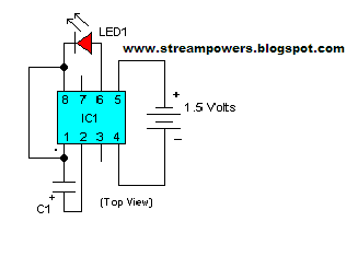
Led Flasher with the LM3909 IC streampowers

The LM3909 is an integrated circuit (IC) which will flash a light-emitting diode (LED). Using only two extra components and a battery, the circuit is cheap and has a very low current drain from a 1.5 V cell.
The circuit can be used as a novelty flasher, an indicator for a dummy alarm bell box, or it could be attached to a torch so that it could be found easily in the dark! The simple circuit
Led Flasher with the LM3909 IC Diagram
Assembly
The circuit can be built on a small piece of Veroboard (the piece shown in Figure 2 measures 15 holes by 10 strips). Using such a board, follow these instructions.

1. Depending on how far away you want the LED from the circuit board, solder a length of insulated wire to each lead of the LED. Use different colours of insulation – say, red and black, connecting the red lead to the anode (a) lead (the longer one) of the LED, and the black one to the cathode (k). Figure 2 shows these leads.
2. Cut the copper tracks as shown in Figure 2, using a 3 mm (1⁄8 inch) diameter drill, rotated between thumb and forefinger, or use the proper tool. Make absolutely sure that the tracks are completely broken!
3. Fit the IC holder in the correct position, using the cut tracks as guides, and make sure the small notch is facing towards the top of the board. Solder the pins to the copper tracks.
4. Mount the capacitor, positive end to the left, so that the positive lead is soldered to track F, which connects it to pin 2 of the IC; the negative lead is soldered to the right-hand side of track E, this being connected to pin 8 of the IC.
5. Solder on the battery leads, positive to the right, and the extended LED leads, positive downwards.
6. Check the circuit, and hold up the board to a bright light and look carefully for solder bridges between the tracks and pieces of copper swarf which may have escaped your inspection in 2 above! Remove whatever you find.
7. When all seems well, put the IC into the socket, ensuring that the notch or dot on the upper surface of the IC lines up with the notch on the holder. Line up each pin on the IC with the hole below it before pressing gently on the IC with the board supported on a firm surface.
8. Connect the battery; the LED should start to flash. The circuit is complete and working!
If you prefer, the whole circuit (battery included) can be mounted in a small plastic box, with the LED mounted on a clip and protruding through the panel. There are many other possibilities, and it is up to you to find an application for your own use.

Parts list
LM3909 Integrated circuit
IC socket 8-pin DIL BL17T
LED 5 mm diameter WL27E
100 microfarad (#F) Electrolytic capacitor (10 V) FB48C
Battery holder For AA-size cell YR59P
Battery 1.5 V AA cell
Small piece of Veroboard (15 holes by 10 strips)
Small plastic box (if required)
LED clip (if required)
Two lengths of coloured, insulated wire for LED (as required)
Read More..

Thursday, February 6, 2014

Tips assembling high quality power amplifier

high quality power amplifier
Amplilfier power series from the beginning until now did not experience any changes. Some say this series is good, but the series was good fitting assembly and tested the results are not as we expected.


The problem is usually treble is less subtle, less sound, sound breaking, buzz, middle of the field tested the bass sound is lost. so you do not have to believe what people 100%. The quality amplifier built-up would differ greatly with the amplifier assembly, a series can be the same but the quality will depend on who manufacture it.

Here are a few tricks to try

How to cope with a buzzing sound 
Power amplifiers are often used in the field blazer. This circuit is said said person is a bell assembly. But you do not immediately interested in this power, the circuit rather complicated and difficult to understand reflect the intelligence of people who first mendisainnya. In my opinion a great power is the power of simple, inexpensive, easily assembled and rational. You do not need to use expensive components such as the price of tantalum capacitors, power mosfet and the other expensive. This does not determine the quality of the power amp so that we raft. Power of sometimes causing buzzing, to overcome that is by holding the line input jack ground to the ground with 10-22 ohm resistors. So do not just take the ground input from the ground but held first with the R 10 ohms.


How to setting bias trimpot
Rotate the trimpot bias (if any) until the drain current of 50-100mA on each power transistor, in order to avoid defects treble in volume in the top position at 10. The risks are so panassss heatsink! (This setting marks on plate A-AB)

Offset trimpot setting
At the time of input without a signal, turn the trimpot so that the voltage on the speaker offsets actually read 0 volts. If you do not want to bother, use and entrust it with ic type series from Hitachi HA17741 IC brand quality or other! This is the heart of the series, 90-95% of quality is determined from the IC circuit this!

Overcoming the voice
Use pre-amp circuit to increase the signal of at least 2 times. normally and should pre-amp circuit uses IC op-amps with +12 V minimum supply-12V. Raise his mid tone!
Kalalu susah2 you do not want to just use the tone control circuit IC is his mid!
The secret is not in his mid tone alone, but the signal output from the IC op-amps are usually large.

Treble rupture
Excessive treble will damage the power amp, power rather than out even ngedrop. Handle, attach the filter capacitor on the input 1NF power amp to ground to ensure the signal is not disabled. Always use a quality active components such as ICs and transistors, 500 price difference will also be different results.
Use a large cable and short as possible, especially for leg power transistor, and this transistor should be directly soldered to the pcb.

Missing bass in field
Usually power for field use supplay CT 50V 50V transformer, or at least 42V 42V ct. The greater the greater the supply voltage watt channeled though the series is written only 300-400 Watts only. This course uses Elko capacitors with voltage 80-100V. 10.000uF/100V capacitor will be equal to 4X10.000uF/50V and of course voltage capacitor is filled with full / almost full.
Try to use a strong Elko at temperatures of 105 C. Capacitors are strong in supply of more than nominal voltage is written on his body. For example 4700uF/50V 85C capacitor will quickly explode in voltage 51V 85C. And Elko will be strong 105C 4700uF/50V voltage supplied more than 50V at a temperature of 85C. Elco so that it does not quickly explode if given the full voltage, keep its temperature as cold as possible, fan with the cool air.

For speaker
Try using a driver speakers that have a large spool diameter fitted with a suitable size bok. Usually included examples of the parameters / dimensions bok. Size bok bok2 usually larger than that sold in the market. if you force using bok that from this market, use driver type G12-80 (sorry no fear brand called promotion) speakers with bass tones to wall size small. Bok wall should be thick, strong and do not forget glued! Bok who will not be glued with a different sound, especially bass tones, prove it!

Heat Sensor
The form of transistor, the transistor is usually type BD139 MJE340 or it could be located in the center, flanked by a pair of transistors having a certain equal. These transistors must be mounted on the main heatsink to detect the heat generated by power transistors. It acts to lower bias currents at the hot heatsink. So what heatsink and power transistors must be set diposisi hot? Yes objectives nothing to prevent the signal from the defect (in class A or AB), with consequent heat. This class is not necessary and will not be felt if you only want the bass tones only. Goal setting on. AB grade is still crystal clear sound even though the maximum volume positioned rotated (in the middle of the field).
It is unlikely, but its closer.

Large heatsink
Not only electrolytic capacitors are more explosive at high temperatures, power transistors can also break away under stress break the original. For example 2SC5200 transistors have the break voltage of 230Vdc, but if temperaturya high voltage values ​​will break his fall well below this value, resulting in faster transistor is damaged. Use of heatsink and cooling fan is very important not only to reduce the heat, more than it can prevent the transistor from break / damaged and weakened output. Increasingly hot temperatures will be more or less ability. Use of this cooling is expected for the components remain fresh, fit and durability.


Choice Component
Power Transistor
There are so many types and models of these transistors, for example MJ15003 MJ15024-4 and-5 from Motorola, but unfortunately these components are not manufactured by Motorola again but from ON semiconductor. Transistor model jengkol usually stronger in the high temperature, probably due to more airtight. 2SC5200 from Toshiba, this transistor is equal dalamannya Sanken 2SC2922 Korea, and both will break if the temperature is too hot. 2SC2922 Sanken issued tin granules when heated, this weakness, the Japanese technology is better than Korean technology. 2SC3281, this transistor is the most popular and frequently used in professional amplifier, but Toshiba does not produce much, if still there in the market, then it most likely is fake!

Transfomer
There are two models of the transformer which is often used, namely EI model (box / conventional) and the model toroid (ring / donut). Some say the toroid transformer model is better because it has a smaller flux kobocoran, in fact the same. Circuits that are sensitive to this flux is high berpenguatan circuits like pre-amp head and mic pre-amp. The circuit is usually installed horizontally / flat parallel to the structure of a conventional transformer wire so that a series of emails received reverberation is greater. Unlike the model toroid transformer is arranged in a vertical wire their email so that the wires are perpendicular to circuit kits The effect is the flux of the pre-amp kit receive a smaller head. To solve for this flux does not enter the series is by downloading shelding / fortified with non-magnetic plate such as aluminum plate and copper plate / sheet pcb board. Plate is of course connected to ground via a cable. To match the flux in a vertical transmission, the conventional transformer needs to be installed side (the side be side down) so that the arrangement of transformer wire stand upright, this method is often used in built-up POWER2. Voltage 50V 50V CT can be obtained by combining the two transformer 25VCT25V, CT is not used, the foot 25V 50V so that the legs be made only to CT, bringing the total number is 100V or 50VCT50V. It deserves used for pwr amp powerless over 400Watt.

Resistor 5 Watt
Resistor on the power transistor legs are usually valued at 0.5 ohm 5 Watt white square. If we dismantle dalamannya it appears there was a circular aluminum wire. It resembles the inductor, the inductive reactance inductor will be higher when fed a high-frequency fractions so that treble tone will be weakened and deformed. Power required to remove the high notes (treble) of course greater, there is a problem here. The use of R 0.5/5W on its home-based power amplifier ok-ok only. But often do not realize the cause of damage to the speakers and power amplifiers is the high treble tones. Treble is not out but was hit by a pwr amp so arising is hot and damaged. We recommend using common Watt resistor 2 12:47 - 1 ohm parallel 2 so that counted 4 Watt. Or if you use 0:22 ohm 2 Watt Resitor unnecessary because the voltage clamp diparalel quite half (one R 0.5/5W replaced one R 0.22/2W) its ok.

Fuse
Nature damage to semiconductor materials / transistor power amplifier is short, if you use a supply that is high enough then the destruction of these transistors will invite their partners to be damaged as well. In order for the destruction of this transitor congregation not need the installation of fuses. 1.5A per power transistor is considered sufficient.
Read More..

Positive Voltage Regulators Datasheets Free Download

DownloadDescriptionSize
78xx series3 Terminal Positive Voltage Regulator +5V until +24V1A229 KB
78Lxx series3 Terminal Positive Voltage Regulator +5V until +24V 0.1A186 KB
78Mxx series3 Terminal Positive Voltage Regulator +5V until +24V 0.5A204 KB
78Sxx series3 Terminal Positive Voltage Regulator +5V until +24V 2A263 KB
Read More..

Stereo Balance Indicator

This stereo balance indicator circuit diagram is designed using few common external components .The schematic circuit is very simple to build and will provide an visual indication with LEDs for left , right and center balance . 

Stereo Balance Indicator Circuit Diagram

 Stereo Balance Indicator Circuit Diagram

Outputs from each channel are fed to the two inputs of IC1 connected as a differential amplifier . Output of the IC1 is connected to the noninverting inputs of the IC2 and IC3 . If the outputs of the IC1 approaches the supply rail , the outputs of the IC2 and IC3 will go high illuminating the LED 3 , this will show that the right channel is dominating . If the sound is balanced to the left channel , the Ic2 and IC3 will go low and the LED1 will light . If both channels are equal in amplitude the outputs of the IC2 and IC3 would be low and high respectively , lighting up LED2 .


Read More..