Showing posts with label 5. Show all posts
Showing posts with label 5. Show all posts
Thursday, September 18, 2014
Inductorless 3 to 5 Volts Converter
By configuring a comparator and a transistor to control the oscillator in a charge pump circuit, you enable the pump to generate a regulated output of in principle any desired value. Charge pump ICs can either invert or double an input voltage (for example, 3 V to –3 V or 3 V to 6 V). The charge pump itself does not regulate the output voltage and one running off 3 V is not normally capable of generating intermediate output voltage levels like 5 V. However, by adding a comparator and a reference device, you can create arbitrary output levels like 5 V and regulate them as well.
Circuit diagram :
Inductorless 3-to-5 Volts Converter Circuit Diagram
Charge pump IC1 (a MAX660) has an internal oscillator whose 45 kHz operation transfers charge from C1 to C2, causing the regulated output to rise.
When the feedback voltage (pin 3 of IC2) exceeds 1.18 V, the output of comparator IC2 (a MAX921) goes high, turning off the oscillator via T1. The comparator hysteresis (easily added on IC2) is zero here simply because no hysteresis is required in the control loop. The oscillator when enabled generates two cycles, which is sufficient to drive VOUT slightly above the desired level. Next, the feedback turns the oscillator off again.
The resulting output ripple will depend mainly on the input voltage and the output load current. Output ripple may be reduced at the expense of circuit efficiency by adding a small resistor (say, 1 ?) in series with C1. You’ll find that ripple also depends on the value and ESR associated with C1 - smaller values of C1 transfer less charge to C2, producing smaller jumps in V OUT.
Author: D. Prabakaran

Saturday, February 8, 2014
5 1 surround amplifier circuit schematic
This 5.1 surround amplifier circuit schematic use the IC AN7168 as the main component from this circuit . Minimum voltage required 12V and maximum voltage 24V , I recomended it 12 V because the voltage support on are components. But if you want to better a loud sound you can raise it.
Maximum power output 40W with impedance 4 ohm . This 5.1 surround amplifier circuit schematic also support to make surround sound or 5.1 speaker. Use this amplifier on rear speaker , left right , and center but dont use to subwoofer speaker. See 5.1 surround amplifier circuit schematic below :
 |
| Click to view large |
If you want to make a 5.1 surround sound you must make 5 the circuit of 5.1 surround amplifier circuit schematic , for left and right speaker , rear left and right speaker , and center speaker. Use the subwoofer speaker with support amlplifier subwoofer circuit .
Friday, December 13, 2013
2 X 2 4 2 x 4 5 17 Watt Power Amplifier
Amplifier circuit here is all based on the ic in the gains. Three IC TA7230P, TA7236P, TA7237AP is intregated circuit (IC) which was applied to the power amplifier. Each IC has a different output, different input voltage, all IC TA7230P, TA7236P, TA7237AP is manufactured by Toshiba.
Read More..
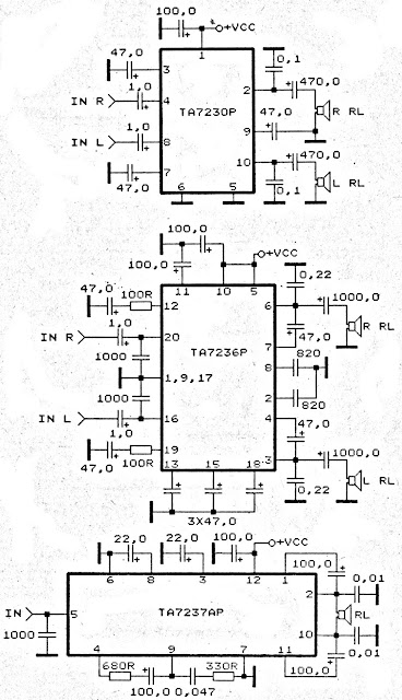 |
TA7230P, TA7236P, TA7237AP amplifier schematic |
Subscribe to:
Posts (Atom)