Showing posts with label circuit. Show all posts

Friday, October 24, 2014

Ni Cd and Ni MH Adjustable constant current Circuit Diagram

This is a battery charger circuit with adjustable current for Ni-MH or Ni-Cd. It can be used for a constant current power, which can be set to any value from a few milliamps to about 500 mA. The maximum current is 500 mA, because that is the limit of transistor BC140. The input voltage must be above 5.25V output voltage, this is due to losses as 1.25V current limit and approximately 4V regulator.

 Battery Charger Ni-Cd and Ni-MH Adjustable constant current Circuit Diagram


The LM317 regulator is used, it should have a sink.

Components
R1 100Ω resistor
VR1 trimpot or potentiometer 500Ω
Capacitor C1 0.1μF
C2 Capacitor 0.01μF
Diode D1 1N4001
Q1 Transistor BC140
IC1 Voltage Regulator LM317
Read More..

Simple Water Level Indicator Circuit Schematic

The whole project was developed on a friends request. Its purpose was to remotely monitor the water-level in a metal tank located in the attic by means of a very simple control unit placed in the kitchen, some floors below.
Mains requirements were:
  1. No separate supply for the remote circuit
  2. Main and remote units connected by a thin two-wire cable
  3. Simple LED display for the main unit
  4. Battery operation to avoid problems related to mains supply and water proximity
  5. As the circuit was battery operated a low current consumption was obviously welcomed
The very small remote unit is placed near the tank and measures the water level in three ranges by means of two steel rods. Each range will cover one third of the tank capacity:

Almost empty - signaled by means of a red LED (D3) in the control unit display
About half-level - signaled by means of a yellow LED (D2) in the control unit display
Almost full - signaled by means of a green LED (D1) in the control unit display

Circuit diagram:

Water-level Indicator Circuit Diagram

Circuit operation:

When the water-level is below the steel rods, no contact is occurring from the metal can and the rods, which are supported by a small insulated (wooden) board. The small circuit built around IC1 draws no current and therefore no voltage drop is generated across R5. IC2A, IC2B and Q1 are wired as a window comparator and, as there is zero voltage at input pins #2 and #5, D3 will illuminate. When the water comes in contact with the first rod, pin #13 of IC1 will go high, as its input pins #9 to #12 were shorted to negative by means of the water contact.

Therefore, R4 will be connected across the full supply voltage and the remote circuit will draw a current of about 9mA. This current will cause a voltage drop of about 0.9V across R5 and the window comparator will detect this voltage and will change its state, switching off D3 and illuminating D2. When the water will reach the second rod, also pin #1 of IC1 will go high for the same reason explained above. Now either R3 and R4 will be connected across the full supply voltage and the total current drawing of the remote circuit will be about 18mA.

The voltage drop across R5 will be now about 1.8V and the window comparator will switch off D2 and will drive D1. The battery will last very long because the circuit will be mostly in the off state. Current is needed only for a few seconds when P1 is pushed to check the water-level and one of the LEDs illuminates.

Parts:

R1 = 15K 1/4W Resistors
R2 = 15K 1/4W Resistors
R3 = 1K 1/4W Resistors
R4 = 1K 1/4W Resistors
R5 = 100R 1/4W Resistor
R6 = 47K 1/4W Resistor
R7 = 3.3K 1/4W Resistors
R8 = 3.3K 1/4W Resistors
R9 = 2.7K 1/4W Resistors
R10 = 15K 1/4W Resistors
R12 = 15K 1/4W Resistors
R13 = 3.3K 1/4W Resistors
R14 = 2.7K 1/4W Resistors
R15 = 2.7K 1/4W Resistors
D1 = 3mm Green LED
D2 = 3mm Yellow LED
D3 = 3mm Red LED
C1 = 470nF 63V Polyester or Ceramic Capacitor
J1 = Two ways output sockets
J2 = Two ways output sockets
P1 = SPST pushbutton
B1 = 9V PP3 Battery
Q1 = BC547 45V 100mA NPN Transistor
IC1 = 4012 Dual 4 input NAND gate IC
IC2 = LM393 Dual Comparator IC
Two steel rods of appropriate length
Read More..

8 Amp Regulated Power Supply circuit Diagram

This power supply is powered by a transformer operating from 120 Vac on the primary and providing proximately 20 Vac on the primary, and providing approximately 20 Vac on the secondary. Four 10-A diodes with a 100 PIV rating are used in a full-wave bridge rectifier.

 8-Amp Regulated Power Supply Circuit Diagram


8-Amp Regulated Power Supply circuit Diagram

A 10,000 ^F/36 Vdc capacitor completes the filtering, providing 28 Vdc. The dc voltage is fed to the collectors of the Darlington connected 2N3055s. Base drive for the pass transistors is from pin 10 of the µ723 through a 200 ohm current limiting resistor, Rl. The reference terminal (pin 6) is tied directly to the non-inverting input of the error amplifier (pin 5), providing 7.15 V for comparison. Link

The inverting input to the error amplifier (pin 4) is fed from the center arm of a 10 k ohm potentiometer connected across the output of the supply. This control is set for the desired output voltage of 13.8 V. Compensation of the error amplifier is accomplished with a 500 pF capacitor connected from pin 13 to pin 4. If the power supply should exceed 8 A or develop a short circuit, the µ723 regulator will bias the transistors to cutoff and the output voltage will drop to near zero until the short circuit condition is corrected.
Read More..

Discrete Virtual Ground Circuit Diagram

Here is the simple virtual ground circuit based on discrete components. This simple design comes from miniaturization guru Sijosae. Is to make a buffer from generic discrete components. The transistors can be most any complementary pair of small-signal transistors. Suitable alternatives are the PN2222A and PN2907A. The diodes are generic small-signal types. An acceptable alternative is the 1N914. This circuit has better performance than a simple resistive divider virtual ground, and the parts cost is lower than for any other circuit mentioned here. It is, however, the least accurate of the buffered virtual ground circuits.

 ircuit diagram:
 
 
 Parts:

R1,R2 = 4.7K
R3,R4 = 4.7R
C1,C2 = 470uF-25V
C3,C4 = 47uF-25V
D1,D2 = 1N4148
Q1 = 2SC1384
Q2 = 2SA684
B1 = Battery
Read More..

Monday, October 20, 2014

Build a Period To Voltage Converter Circuit Diagram

this is the simple Period To Voltage Converter Circuit Diagram. The input signal drives ICD. Because ICD`s positive input (V+) is slightly offset to + 0.1 V, its steady state output will be around +13 V. This voltage is sent to ICC through D2, setting ICC`s output to +13 V. Therefore, point D is cut off by Dl, and CI is charged by the current source. 

Assuming the initial voltage on CI is zero, the maximum voltage (^Cinax) is given by: When the input goes from low to high, a narrow positive pulse is generated at point A. This pulse becomes -13 V at point B, which cuts off D2. ICC`s V+ voltage becomes zero. 

Period To Voltage Converter Circuit Diagram

Period To Voltage Converter Circuit Diagram

The charge on CI will be absorbed by ICC on in a short time. The time constant of C2 and R5 determines the discharge period— about 10 /is. ICB is a buffer whose gain is equal to (R& + R9)~Rg = lM5. ICD`s average voltage will be (1362f 1.545) + 2 = 1052/. RIO and C3 smooth the sawtooth waveform to a dc output.
Read More..

Photo Electric Street Light Circuit Diagram

This is basically a Schmitt Trigger circuit which receives input from a cadmium sulfide photo cell and controls a relay that can be used to switch off and on a street lamp at dawn and dusk. I have built the circuit with a 120 ohm/12 volt relay and monitored performance using a lamp dimmer, but did not connect the relay to an outside light.

The photo cell should be shielded from the lamp to prevent feedback and is usually mounted above the light on top of a reflector and pointed upward at the sky so the lamp light does not strike the photo cell and switch off the lamp.

Photo Electric Street Light Circuit Diagram

Lights Circuit Diagram
 
The photo cell is wired in series with a potentiometer so the voltage at the junction (and base of transistor) can be adjusted to about half the supply, at the desired ambient light level. The two PNP transistors are connected with a common emitter resistor for positive feedback so as one transistor turns on, the other will turn off, and visa versa. Under dark conditions, the photo cell resistance will be higher than the potentiometer producing a voltage at Q1 that is higher than the base voltage at Q2 which causes Q2 to conduct and activate the relay.

The switching points are about 8 volts and 4 volts using the resistor values shown but could be brought closer together by using a lower value for the 7.5K resistor. 3.3K would move the levels to about 3.5 and 5.5 for a range of 2 volts instead of 4 so the relay turns on and off closer to the same ambient light level. The potentiometer would need to be readjusted so that the voltage is around 4.5 at the desired ambient condition. Link
Read More..

Simple Mat Switch Circuit

This simple Simple Mat Switch Circuit Diagram produces a warning beep when somebody crosses a protected area in your home or office. The switch, hidden be-low the floor mat, triggers the alarm when the person walks over it.

The circuit uses a conductive foam as the switch. It can be two small pieces of conductive pads usually used to pack sensitive ICs as antistatic cover. Alternatively, you can make the switch by coating conducting carbon ink on two small pieces of a copper-clad board.

Circuit diagram :

Link


Simple Mat Switch Circuit Diagram

When the circuit is in standby mode, transistor T1 does not conduct, since its base is floating. When the person walks, the switch is pressed and current flows through R1 and the switch to provide positive bias to transistor T1. Transistor T1 conducts and its collector voltage drops, which acts as a negative trigger input for the monostable wired around IC NE555 (IC1).

IC1 outputs a pulse of fifty-seconds duration with preset values of R4 and C3. This pulse is applied to the buzzer through transistor T2. The buzzer sounds a warning beep on unauthorised entry. The pulse duration can be changed to the desired value by changing the values of R4 and C3. Resistor R2 in the circuit makes the trigger pin of IC1 high to prevent false triggering.

Assemble the circuit on a general-purpose PCB and enclose in a plastic case. Use a 9V battery to power the circuit. Connect the touchpad switch with the PCB and hide under the mat at the entrance. The PCB can be mounted on the nearby wall.

Make the switch carefully using conducting foam or copper clad coated with conducting ink. Place the two pieces with their conducting surface facing each other. Solder carefully a thin copper electric wire and ensure that it makes contact when the two plates touch together on pressing. Provide two 1cm rubber tabs between the plates to avoid touch in the standby mode.
Read More..

Simple Solar Engine Circuit Diagram

 Simple Solar Engine Circuit Diagram
 
Simple Solar Engine Circuit Diagram Small DC motor runs off of calculator solar cell in dim light. How do we achive 10nA operation? By using diodes in place of pull up resistors, and by isolating the DC load from the trigger circuit via junction drops and the 10nF capacitor. If there is too much power comming from the solar cell then the motor might run too often or even continuously. You can avoid this by putting a 100K ohm resistor in series with the solar cell. 

 Simple Solar Engine Circuit Diagram

 Simple Solar Engine Circuit Diagram

Read More..

Friday, October 17, 2014

Build a Simple Audio Amplifier 2800W Circuit Diagram

How to Build a Simple Audio Amplifier 2800W Circuit Diagram. This is a Mono high power amplifier is actually a powerful 1400 W, but if this high power amplifier circuit is doubled and you want to create stereo, high power amplifier the necessary components and pcb requires two-fold. So if the stereo high power amplifier 2 X 1400W. Schematic Circuit diagram is still less by looking at the circuit that was so below, the finished circuit has been added with a gains using JRC4558 IC by the two and the picture ic where it can be seen below. 

For circuit buffers, drivers, and booster use multiple transistors and other components (can be seen listed component). And high power amplifier project that is so below is just part of the buffer and driver while the booster has not been made​​. For additional transistors in the booster or high power amplifier end scheme can be found Booster output power amplifier.

 Audio Amplifier 2800W Circuit Diagram


Part List :

Resistor
R1_____560Ω
R2_____100Ω
R3_____2K2Ω
R4_____560Ω
R5_____1Ω
R6_____27KΩ
R7_____10KΩ
R8_____100Ω
R9_____100Ω
R10____100Ω
R11____12KΩ
R12____100Ω
R13____100Ω
R14____100Ω
R15____27KΩ
R16____2K2Ω
R17____560Ω
R18____100Ω
R19____10KΩ
R20____330Ω
R21____47Ω 2W
R22____56Ω
R23____2K2Ω
R24____22Ω
R25____56Ω
R26____180Ω
R27____500-1KΩ Trim
R28____560Ω
R29____56Ω
R30____56Ω
R31____22Ω 1W
R32____5Ω6 2W
R33____10Ω
R34____180Ω
R35____100Ω
R36____22Ω 2W
R37____180Ω
R38____56Ω
R39____47Ω 2W
R40____5Ω6 2W
R41____10Ω
R42____10Ω
R43____10Ω
R45____10Ω
R46____0.22Ω 5W
R47____0.22Ω 5W
R48____0.22Ω 5W
R49____0.22Ω 5W
R50____10Ω 5W

Capacitor
C1_____1цF
C2_____1.5nF
C3_____0.1цF 250-275V
C4_____0.1цF 250-275VC5_____100nF
C6_____100цF 50V
C7_____39pF
C8_____330pF
C9_____330pF
C10____330pF
C11____47nF 250-275V
C12____220nF 250-275V

Transistor
T1_____MJE340
T2_____2N5551 / C2240
T3_____2N5551 / C2240
T4_____2N5551 / C2240
T5_____2N5551 / C2240
T6_____2N5401 / BF423
T7_____2N5401 / BF423
T8_____2N5401 / BF423
T9_____2N5401 / BF423
T10____MJE350
T11____B1186
T12____TIP127
T13____D1763
T14____D1763
T15____B1186
T16____C5198
T17____A1941
T18____2SC2922 / MJ15024G
T19____2SC2922 / MJ15024G
T20____2SA1216 / MJ15025G
T21____2SA1216 / MJ15025G


Sourced by SIGMA-4 Madiun ©
Read More..

Saturday, October 11, 2014

Low Power Voltage Doubler Circuit Diagram

All miniature electronic devices operate off batteries. Some of them need higher than the standard battery voltages to operate efficiently. If the battery of that specific voltage is unavailable, we are forced to connect additional cells in series to step up the DC voltage. Thus, the true meaning of miniaturisation is lost. A simple way to overcome this problem is to employ a voltage doubler, if the device under consideration can operate at a small current.

Here we present a low-power voltage doubler circuit that can be readily used with devices that demand higher voltage than that of a standard battery but low operating current to work with. The circuit is quite simple as it uses only a few components. Yet, the output efficiency is 75 to 85 percent along its operating voltage range. The available battery voltage is almost doubled at the output of the circuit.

Here IC1 is wired as an astable multivibrator to generate rectangular pulses at around 10 kHz. This frequency and duty cycle of the pulses can be varied using preset VR1. The pulses are applied to switching transistors T1 and T2 for driving the output section, which is configured as a voltage-doubling circuit. The doubled voltage is available across capacitor C5. During each cycle of the pulse occurance, the high level drives T1 into its saturation, keeping transistor T2 cut off.

Circuit diagram:

Low-Power Voltage Doubler Circuit Diagram

So transistor T1 charges capacitor C4 via the path formed by diodes D2 and D1 to a voltage level slightly lesser than the supply. But during the low period of the pulse, transistor T1 is cut off while transistor T2 is driven into saturation. Now, transistor T2 raises the charge on the negative pole of capacitor C4 by another step equal to the supply voltage. Therefore an equal amount of charging is built up on capacitor C5 via diode D3.

This doubling action increases the total voltage across capacitor C5 to almost double the input voltage. If the output of the pulse generator is maintained with a high enough amplitude and frequency, the output voltage and current remain constant and cater to the needs of the load. Even with the half-wave function, this circuit is almost free of ripple voltage. If the connected load doesn’t require a high current, the efficiency can be expected in the upper 90 percentranges.

Since the input voltage is doubled, the current drain from the input power supply is also doubled at the input but halved at the output. One point of caution is that if the multivibrator’s frequency is fairly high, the output may suffer with the interference imposed over the DC voltage. In this case, the frequency must be set favorably by trials and actual load connection procedure. This tiny circuit can be assembled on the general-purpose PCB. If all of the components are surface-mount type, the whole module can be genuinely miniaturized.

EFY Lab note. During testing with input of 8V and 1.25mA load current the output voltage was found to be around 13V.

Author :M.K. Chandra ,Mouleeswaran And A.N. Vadivudai Naayaki
 
 
Source
: www . efymag . com
Read More..

Wednesday, February 26, 2014

Multitasking Pins Circuit

It’s entirely logical that low-cost miniature microcontrollers have fewer ‘legs’ than their bigger brothers and sisters – sometimes too few. The author has given some consideration to how to economise on pins, making them do the work of several. It occurred that one could exploit the high impedance feature of a tri-state output. In this way the signal produced by the high impedance state could be used for example as a CS signal of two ICs or else as a RD/ WR signal. 

Circuit diagram:
multitasking pins circuit diagram Multitasking Pins Circuit Diagram

All we need are two op-amps or comparators sharing a single operating voltage of 5 V and outputs capable of reaching full Low and High levels in 5-V operation (preferably types with rail-to-rail outputs). Suitable examples to use are the LM393 or LM311.The resistances in the voltage dividers in this circuit are uniformly 10 kilo ohms. Consequently input A lies at half the operating voltage (2.5 V), assuming nothing is connected to the input – or the microcontroller pin connected is at high impedance. 

The non-inverting input of IC1A lies at two thirds and the inverting input of IC1B at one third of the operating voltage, so that in both cases the outputs are set at High state. If the microcontroller pin at input A becomes Low, the output of IC1B becomes Low and that of IC1A goes High. If A is High, everything is reversed.
Read More..

Sunday, February 9, 2014

Headphone amplifier circuit

Headphone amplifier circuit with op amp ic OPA134, 2134, NE5532, 5534.
Headphone amplifier circuit
Headphone amplifier circuit with op amp
Read More..

AVR Dongle Circuit

This circuit is intended to program AVR controllers such as the AT90S1200 via the parallel port. The circuit is extremely simple. IC1 provides buffering for the signals that travel from the parallel port to the microcontroller and vice versa. This is essentially everything that can be said about the circuit. The two boxheaders (K2 and K3) have the ‘standard’ ISP (in system programming) pinout for the AVR controllers. The manufacturer recommends these two pinouts in an attempt to create a kind of standard for the in-circuit programming of AVR-controllers. These connections can be found on many development boards for these controllers. The software carries out the actual programming task.

Circuit diagram :
AVR_Dongle_Circuit_Diagramw
AVR Dongle Circuit Diagram

It is therefore necessary to have a program (ATMEL AVR ISP), which is available as a free download from http://www.atmel.com. The construction of the circuit will have to made on standard prototype board, since we didn’t design a PCB for this circuit. This should not present any difficulties considering the small number of parts involved. We recommend that inexperienced builders first make a copy of the circuit and cross off each connection on the schematic once it has been made on the board. This makes it easy to check afterwards whether all connections have been made or not.

http://www.ecircuitslab.com
Read More..

10 Watt Power Amplifier Circuit

IC BA514 its the main of  this circuit. This is actually low power output with minimum power output 2 W but maximum output 10W . Minimum voltage require 9 Volt and maximum voltage 14 Volt . Impedance output 4 Ohm.
Power Amplifier Schematic below :


Click to view Larger
All capacitor with uF and minimum voltage capacitor is 16 V. resistor with 1/4 Watt.
Read More..

Saturday, February 8, 2014

5 1 surround amplifier circuit schematic

This 5.1 surround amplifier circuit schematic use the IC AN7168 as the main component from this circuit . Minimum voltage required 12V and maximum voltage 24V , I recomended it 12 V because the voltage support on are components. But if you want to better a loud sound you can raise it. 

Maximum power output 40W with impedance 4 ohm . This 5.1 surround amplifier circuit schematic also support to make surround sound or 5.1 speaker. Use this amplifier on rear speaker , left right , and center but dont use to subwoofer speaker. See 5.1 surround amplifier circuit schematic below :

Click to view large
If you want to make a 5.1 surround sound you must make 5 the circuit of 5.1 surround amplifier circuit schematic , for left and right speaker , rear left and right speaker , and center speaker. Use the subwoofer speaker with support amlplifier subwoofer circuit .


Read More..

Solid State Relay Circuit Diagram

Solid State Relay Circuit
Solid state relay is a series that functions like a relay hibryd mechanics. Solid state relays is built with insulating an MOC for separate the input and the switch. With Solid state relays we can avoid the occurrence of sparks as it did in the relay can also avoid the occurrence of conventional connection is not perfect because porous contactor as in conventional relays.


The series of solid state relays This is quite simple and we can make in a PCB hole. For more details can be seen in the picture following a series of solid state relays.

Solid State Relay Circuit
Solid State Relay Circuit Diagram

Solid state relay has many advantages including no mechanical friction on the contactor, the connection process only occur when there are crosses zero, there is no spark at the contactor, not noisy, small konsusi flow control, better endurance.
Read More..

Thursday, February 6, 2014

High impedance balance output circuit

Because of high input impedance required to maximize CMRR, High impedance balance output circuit shown in figure below , has been used for the input impedance is determined solely by the input bias resistance R1 and R2. High impedance balance output circuit also useful for interfacing with valve equipment in the strange world of retro-hi-fi.
high impedance schematic
High impedance balance output circuit
Adding the output cathode followers for valve circuits are expensive and consume a lot of extra energy, so that the output is often taken directly from the anode gain-stage, as a result, even loading bridge the so-called 10 k distortion can seriously endanger performance and output swing available from the source equipment.
All balanced phase dealt with until now have their input impedance is determined by value input resistors, etc., and this can not be raised without lowering the noise performance.
High impedance balance output circuit diagrams above shows one answer to this. Input op-amp itself is quite a lot has infi nite
Impedance in terms of audio, so the input impedance is determined by the need to R1, R2 bias non-inverting input. A property of remarkable and very useful from this circuit is that the addition of Rg resistance increased profits, but maintain the balance of the circuit. This confidentiality guration can not be set to weaken for the advantages of an op-amp with feedback on the series can not decreases below unity.
Read More..

Wednesday, February 5, 2014

Smoke detector circuit

This causes the resistance of LDR to increase and the voltage at the base of the transistor is pulled high due to which the supply to the COB (chip-on-board) is completed. The sensitivity of the smoke detector depends on the distance between bulb and LDR as well as setting of preset VR1.
Thus by placing the bulb and the LDR at appropriate distances, one may vary preset VR1 to get optimum sensitivity.
We have not build this smoke alarm detector.

For smoke detector installation and maintenance use a near electrician.
Read More..

Tuesday, February 4, 2014

18W Amplifier Schematic Circuit

18W Amplifier Schematic Circuit

18W Amplifier Schematic Circuit Part List

P1_____________22K Log. Potentiometer (Dual-gang for stereo)

R1______________1K 1/4W Resistor

R2______________4K7 1/4W Resistor

R3____________100R 1/4W Resistor

R4______________4K7 1/4W Resistor

R5_____________82K 1/4W Resistor

R6_____________10R 1/2W Resistor

R7_______________R22 4W Resistor (wirewound)

R8______________1K 1/2W Trimmer Cermet (optional)

C1____________470nF 63V Polyester Capacitor

C2,C5_________100µF 3V Tantalum bead Capacitors

C3,C4_________470µF 25V Electrolytic Capacitors

C6____________100nF 63V Polyester Capacitor

D1___________1N4148 75V 150mA Diode

IC1________TLE2141C Low noise, high voltage, high slew-rate Op-amp

Q1____________BC182 50V 100mA NPN Transistor

Q2____________BC212 50V 100mA PNP Transistor

Q3___________TIP42A 60V 6A PNP Transistor

Q4___________TIP41A 60V 6A NPN Transistor

J1______________RCA audio input socket

Power supply parts:

R9______________2K2 1/4W Resistor

C7,C8________4700µF 25V Electrolytic Capacitors

D2_____________100V 4A Diode bridge

D3_____________5mm. Red LED

T1_____________220V Primary, 15 + 15V Secondary, 50VA Mains transformer

PL1____________Male Mains plug

SW1____________SPST Mains switch
Read More..

Tuesday, January 28, 2014

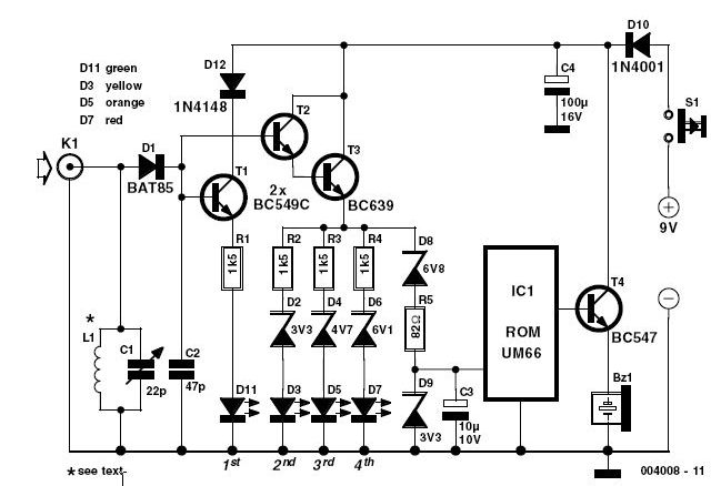
144 MHz Simple RF Detector Circuit

144 MHz Simple RF Detector Circuit
This simple circuit helps you sniff out RF radiation from your transmitter, improper joints, a broken wire or poor equipment with RF shielding. The tester is designed for the radio band amateur 2 meter (144-146 MHz in Europe). The instrument has a reading of 4-step LED and an audible alarm for high voltage radiation. The RF signal is received by an antenna and made to resonate by C1-L1. After rectification by the diode D1, the signal is fed to a two transistor Darlington amplifier HighGain, T2-T3. Assuming a 10-inch telescoping antenna using the RF level scale established for the LEDs is as follows:

When all the LEDs light, the (optional) UM66 sound / melody generator chip (IC1) also operates and provides an audible alarm. By changing the zener diode values ​​of D2, D4, D6 and D8, the step size and duration of the instrument may change as needed. To operate in other bands of ham or PMR, simply change the network-L1 C1 resonance.

For example, a transceiver 5 watt handheld equipped with a telescoping half-wave antenna (G = 3.5 dBd), there is an ERP (Effective Radiated Power) of just 10 watts and an emf of more than 8 volts near the head. Inductor L1 consists of 2.5 turns of 20 SWG (approximately 1 mm in diameter) enameled copper wire. The inner diameter is approximately 7 mm and no core is used.

Trimmer capacitor C1 associates is adjusted for the greatest number of LEDs to light at a relatively low fieldstrength position for a 2 m transceiver 145 MHz transmission. The tester is powered by a 9 V battery and consumes about 15 mA when all LEDs are on. Must be enclosed in a metal box.
Read More..