Showing posts with label audio. Show all posts

Friday, October 24, 2014

Audio Clipping Indicator

Detects clipping in preamp stages, mixers, amplifiers etc., Single LED display - 9V Battery supply unit
This circuit was intended to be used as a separate, portable unit, to signal by means of a LED when the output wave form of a particular audio stage is "clipping" i.e. is reaching the onset of its maximum permitted peak-to-peak voltage value before an overload is occurring. This will help the operator in preventing severe, audible distortion to be generated through the audio equipment chain. 

This unit is particularly useful in signaling overload of the input stages in mixers, PA or musical instruments amplification chains, but is also suited to power amplifiers. A careful setting of Trimmer R5 will allow triggering of the LED with a wide range of peak-to-peak input voltages, in order to suit different requirements. Unfortunately, an oscilloscope and a sine wave frequency generator are required to accurately setup this circuit. Obviously, the unit can be embedded into an existing mixer, preamp or power amplifier, and powered by the internal supply rails in the 9 - 30V range. The power supply can also be obtained from higher voltage rails provided suitable R/C cells are inserted. SW1 and B1 must obviously be omitted.

Circuit diagram:
Audio_Clipping_Indicator_Circuit DIagram
Audio Clipping Indicator Circuit Diagram
Parts:
R1___________1M 1/4W Resistor (See Notes)
R2,R3,R8_____100K 1/4W Resistors
R4,R6________10K 1/4W Resistors
R5___________5K 1/2W Trimmer Cermet or Carbon
R7___________2K2 1/4W Resistor
R9___________22K 1/4W Resistor
R10__________1K 1/4W Resistor (See Notes)
C1,C4________220nF 63V Polyester Capacitors
C2___________4p7 63V Ceramic Capacitor (See Notes)
C3___________220µF 25V Electrolytic Capacitor
C5___________10µF 25V Electrolytic Capacitor (See Notes)
D1,D2________1N4148 75V 150mA Diodes
D3___________LED (Any dimension, shape and color)
Q1___________BC547 45V 100mA NPN Transistor
IC1___________TL062 Dual Low current BIFET Op-Amp (or TL072, TL082)
SW1__________SPST Toggle or Slide Switch (See Text)
B1____________9V PP3 Battery (See Text)

Circuit operation:
The heart of the circuit is a window comparator formed by two op-amps packaged into IC1. This technique allows to detect precisely and symmetrically either the positive or negative peak value reached by the monitored signal. The op-amps outputs are mixed by D1 and D2, smoothed by C4, R7 and R8, and feed the LED driver Q1 with a positive pulse. C5 adds a small output delay in order to allow detection of very short peaks.

Notes:
  • With the values shown, the circuit can be easily set up to detect sine wave clipping from less than 1V to 30V peak-to-peak (i.e. 15W into 8 Ohms). If you need to detect higher output peak-to-peak voltages, R1 value must be raised. On the contrary, if the circuit will be used to detect only very low peak-to-peak voltages, it is convenient to lower R1 value to, say, 220K omitting C2. In this way, the adjustment of R5 will be made easier.
  • Using a TL062 chip at 9V supply, stand-by current drawing is about 1.5mA and less than 10mA when the LED illuminates. With TL072 or TL082 chips, current drawing is about 4.5mA and 13mA respectively.
  • When using power supplies higher than 12V, the value of R10 must be raised accordingly.
  • When using power supplies higher than 25V, the working voltage value of C5 must be raised to 35 or 50V.


http://www.ecircuitslab.com/2011/09/audio-clipping-indicator.html
Read More..

Friday, October 17, 2014

Build a Simple Audio Amplifier 2800W Circuit Diagram

How to Build a Simple Audio Amplifier 2800W Circuit Diagram. This is a Mono high power amplifier is actually a powerful 1400 W, but if this high power amplifier circuit is doubled and you want to create stereo, high power amplifier the necessary components and pcb requires two-fold. So if the stereo high power amplifier 2 X 1400W. Schematic Circuit diagram is still less by looking at the circuit that was so below, the finished circuit has been added with a gains using JRC4558 IC by the two and the picture ic where it can be seen below. 

For circuit buffers, drivers, and booster use multiple transistors and other components (can be seen listed component). And high power amplifier project that is so below is just part of the buffer and driver while the booster has not been made​​. For additional transistors in the booster or high power amplifier end scheme can be found Booster output power amplifier.

 Audio Amplifier 2800W Circuit Diagram


Part List :

Resistor
R1_____560Ω
R2_____100Ω
R3_____2K2Ω
R4_____560Ω
R5_____1Ω
R6_____27KΩ
R7_____10KΩ
R8_____100Ω
R9_____100Ω
R10____100Ω
R11____12KΩ
R12____100Ω
R13____100Ω
R14____100Ω
R15____27KΩ
R16____2K2Ω
R17____560Ω
R18____100Ω
R19____10KΩ
R20____330Ω
R21____47Ω 2W
R22____56Ω
R23____2K2Ω
R24____22Ω
R25____56Ω
R26____180Ω
R27____500-1KΩ Trim
R28____560Ω
R29____56Ω
R30____56Ω
R31____22Ω 1W
R32____5Ω6 2W
R33____10Ω
R34____180Ω
R35____100Ω
R36____22Ω 2W
R37____180Ω
R38____56Ω
R39____47Ω 2W
R40____5Ω6 2W
R41____10Ω
R42____10Ω
R43____10Ω
R45____10Ω
R46____0.22Ω 5W
R47____0.22Ω 5W
R48____0.22Ω 5W
R49____0.22Ω 5W
R50____10Ω 5W

Capacitor
C1_____1цF
C2_____1.5nF
C3_____0.1цF 250-275V
C4_____0.1цF 250-275VC5_____100nF
C6_____100цF 50V
C7_____39pF
C8_____330pF
C9_____330pF
C10____330pF
C11____47nF 250-275V
C12____220nF 250-275V

Transistor
T1_____MJE340
T2_____2N5551 / C2240
T3_____2N5551 / C2240
T4_____2N5551 / C2240
T5_____2N5551 / C2240
T6_____2N5401 / BF423
T7_____2N5401 / BF423
T8_____2N5401 / BF423
T9_____2N5401 / BF423
T10____MJE350
T11____B1186
T12____TIP127
T13____D1763
T14____D1763
T15____B1186
T16____C5198
T17____A1941
T18____2SC2922 / MJ15024G
T19____2SC2922 / MJ15024G
T20____2SA1216 / MJ15025G
T21____2SA1216 / MJ15025G


Sourced by SIGMA-4 Madiun ©
Read More..

Saturday, October 11, 2014

Moduler Audio Preamplifier

High Quality, Discrete Components Models, Input and Tone Control Modules
To complement the 60 Watt MosFet Audio Amplifier a High Quality Preamplifier design was necessary. A discrete components topology, using + and - 24V supply rails was chosen, keeping the transistor count to the minimum, but still allowing low noise, very low distortion and high input overload margin. Obviously, the modules forming this preamplifier can be used in different combinations and drive different power amplifiers, provided the following stages present a reasonably high input impedance (i.e. higher than 10KOhm).
Main Module:
If a Tone Control facility is not needed, the Preamplifier will be formed by the Main Module only. Its input will be connected to some sort of changeover switch, in order to allow several audio reproduction devices to be connected, e.g. CD player, Tuner, Tape Recorder, iPod, MiniDisc etc. The total amount and type of inputs is left to the choice of the home constructor. The output of the Main Module will be connected to a 22K Log. potentiometer (dual gang if a stereo preamp was planned). The central and ground leads of this potentiometer must be connected to the power amplifier input.
Circuit diagram:
Main Module Circuit DiagramMain Module Circuit Diagram
Parts:
R1_____________1K5 1/4W Resistor
R2_____________220K 1/4W Resistor
R3_____________18K 1/4W Resistor
R4_____________330R 1/4W Resistor
R5_____________39K 1/4W Resistor
R6_____________56R 1/4W Resistor
R7,R10_________10K 1/4W Resistors
R8_____________33K 1/4W Resistor
R9_____________150R 1/4W Resistor
R11____________ 6K8 1/4W Resistor
R12,R13________100R 1/4W Resistors
R14____________100K 1/4W Resistor
C1_____________220nF 63V Polyester Capacitor
C2_____________220pF 63V Polystyrene or ceramic Capacitor
C3_____________1nF 63V Polyester or ceramic Capacitor
C4,C7__________47µF 50V Electrolytic Capacitors
C5,C6__________100µF 50V Electrolytic Capacitors
Q1,Q2__________BC550C 45V 100mA Low noise High gain NPN Transistors
Q3_____________BC556 65V 100mA PNP Transistor
Q4_____________BC546 65V 100mA NPN Transistor
Tone Control Module:
This Module employs an unusual topology, still maintaining the basic op-amp circuitry of the Main Module with a few changes in resistor values. A special feature of this circuit is the use of six ways switches instead of the more common potentiometers: in this way, precise "tone flat" setting, or preset dB steps in bass and treble boost or cut can be obtained. Tone Control switches also allow a more precise channel matching when a stereo configuration is used, avoiding the frequent poor alignment accuracy presented by common ganged potentiometers. Six ways (two poles for stereo) rotary switches were chosen for this purpose as easily available. This dictated the unusual "asymmetrical" configuration of three positions for boost, one for flat and two for cut.
This choice was based on the fact that tone controls are used in practice more for frequency boosting than for cutting purposes. In any case, +5dB +10dB and +15dB of bass boost and -3dB and -10dB of bass cut were provided. Treble boost was also set to +5dB +10dB and +15dB and treble cut to -3.5dB and -9dB. Those wishing to use common potentiometers in the usual way for Tone Controls may use the circuit shown enclosed in the dashed box (bottom-right of the Tone Control Module circuit diagram) to replace switched controls. The Tone Control Module should usually be placed after the Main Input Module, and the volume control inserted between the Tone Control Module output and the power amplifier input. Alternatively, the volume control can also be placed between Main Input Module and Tone Control Module, at will. Furthermore, the position of these two modules can be also interchanged.
Circuit diagram:
Tone Control Module Circuit Diagram
Parts:
R1,R7___________47K 1/4W Resistors
R2_____________220K 1/4W Resistor
R3______________18K 1/4W Resistor
R4_____________330R 1/4W Resistor
R5______________39K 1/4W Resistor
R6______________56R 1/4W Resistor
R8_____________150R 1/4W Resistor
R9______________10K 1/4W Resistor
R10,R16__________6K8 1/4W Resistors
R11,R12________100R 1/4W Resistors
R13____________100K 1/4W Resistor
R14______________1K5 1/4W Resistor
R15,R21,R22______4K7 1/4W Resistors
R17,R24,R26______8K2 1/4W Resistors
R18______________3K3 1/4W Resistor
R19______________1K 1/4W Resistor
R20____________470R 1/4W Resistor
R23,R25_________12K 1/4W Resistors
R27,R28__________4K7 1/4W Resistors
C1_____________220nF 63V Polyester Capacitor
C2_______________1nF 63V Polyester or ceramic Capacitor
C3,C6___________47µF 50V Electrolytic Capacitors
C4,C5__________100µF 50V Electrolytic Capacitors
C7______________10nF 63V Polyester Capacitor
C8,C9__________100nF 63V Polyester Capacitors
Q1,Q2_________BC550C 45V 100mA Low noise High gain NPN Transistors
Q3____________BC556 65V 100mA PNP Transistor
Q4____________BC546 65V 100mA NPN Transistor
SW1,SW2_______2 poles 6 ways Rotary Switches
Simpler, alternative Tone Control parts:
P1______________22K Linear Potentiometer
P2______________47K Linear Potentiometer
R29,R30________470R 1/4W Resistors
R31,R32__________4K7 1/4W Resistors
C10_____________10nF 63V Polyester Capacitor
C11,C12________100nF 63V Polyester Capacitors
Power supply:
The preamplifier must be feed by a dual-rail, +24 and -24V 50mA dc power supply. This is easily achieved by using a 48V 3VA center-tapped mains transformer, a 100V 1A bridge rectifier and a couple of 2200µF 50V smoothing capacitors. To these components two 24V IC regulators must be added: a 7824 (or 78L24) for the positive rail and a 7924 (or 79L24) for the negative one. The diagram of such a power supply is the same of that used in the Headphone Amplifier, but the voltages of the secondary winding of the transformer, smoothing capacitors and IC regulators must be uprated. Alternatively, the dc voltage can be directly derived from the dc supply rails of the power amplifier, provided that both 24V regulators are added.
Note:
If this preamplifier is used as a separate, stand-alone device, thus requiring a cable connection to the power amplifier, some kind of output short-circuit protection is needed, due to possible shorts caused by incorrect plugging. The simplest solution is to wire a 3K3 1/4W resistor in series to the output capacitor of the last module (i.e. the module having its output connected to the preamp main output socket).
Technical data:
Main Module Input sensitivity:
250mV RMS for 1V RMS output
Tone Control Module Input sensitivity:
1V RMS for 1V RMS output
Maximum output voltage:
13.4V RMS into 100K load, 11.3V RMS into 22K load, 8.8V RMS into 10K load
Frequency response:
flat from 20Hz to 20KHz
Total harmonic distortion @ 1KHz:
1V RMS 0.002% 5V RMS 0.003% 7V RMS 0.003%
Total harmonic distortion @10KHz:
1V RMS 0.003% 5V RMS 0.008% 7V RMS 0.01% 

Read More..

Thursday, February 27, 2014

Remote Audio Level Indicator

The normal level-indicator circuits which are available in the market require connections to be made to the output of the player, which may not be easily accessible. The audio level indicator circuit described here removes this restriction as it may be placed close to the player’s speakers and yet the desired effect can be realised. 

Circuit diagram :
Remote Audio Level Indicator-Circuit Diagram
Remote Audio Level Indicator Circuit Diagram

As shown in the circuit, signals are picked up by the condenser microphone, which get further amplified by the noninverting amplifier built around one of the four op-amps of LM324. The remaining three, along with four op-amps of the second LM324, are used as seven comparators to work as the level detector, giving seven output levels through seven coloured LEDs. 

The sensitivity of the audio level indicator circuit may be improved by varying the 220k potentiometer. If a fine adjustment is desired, a 4.7-kilohm potentiometer may be connected in series resistors with the 220k potentiometer.


Copyright : EFY
Read More..

Wednesday, February 26, 2014

Clipping Indicator For Audio Amplifiers

A clipping indicator is a useful accessory on any audio amplifier. It indicates when the amplifier has reached its limit and is clipping the peaks of the audio signal. In practice, quite a lot of clipping can occur before you can hear it. So why is it necessary to know when an amplifier is clipping if you cant notice it? The answer is that clipping "squares up" the waveform and square waves contain lots of higher-frequency harmonics which can easily damage the tweeters in loudspeaker systems. This circuit is a true clipping indicator as opposed to the level indicators that are commonly used in preamplifier stages.

The problem with level indicators is that an amplifiers maximum output power is not constant. Thats because the amplifiers supply rails are not regulated and so the maximum power available at any given instant varies, depending on the applied signal. The circuit is quite simple and is based on two BD140 PNP transistors and zener diode ZD1. During normal operation, Q1 is turned on via ZD1 and R1. As a result, Q2 is held off (since its base is pulled high) and so LED1 is also off. However, if the output signal subsequently rises to within 4.7V of the positive supply rail, Q1 turns off since it no longer has any forward bias on its base.

Circuit diagram:
clipping-indicator-for-audio amplifiers
Clipping Indicator Circuit Diagram

As a result Q2s base is now pulled low via R2 and so Q2 turns on and lights LED1. (Note: the 0.6V drop across Q1s base/emitter is ignored here because ZD1 conducts before its rated voltage due to the very low current involved). Why choose 4.7V below the power rail as the turn-on point? The reason is that, due to the drive limitations and the nature of emitter followers, they can be expected to have at least 4V across them when they saturate (ie, clip). ZD1 can be increased to a 5V or 6.2V type if the circuit is to be used with a monster amplifier.

The value of R3 should be customized according to the amplifiers supply rail, so that LED1 operates with the correct brightness. To do that, first measure the amplifiers positive supply voltage, then use Ohms Law (R = V/I) to calculate the value of R3 for a current of about 20mA. As it stands, this circuit can only be used to monitor the positive-going half-cycles of the audio waveform. If you want to monitor the negative half-cycles as well, you will have to build a second circuit with the following changes: (1) reverse both LED1 and ZD1; and (2) use BD139 (NPN) transistors for Q1 & Q2. Note that, in both cases, you should use the earth inside the amplifier, as the speaker negative may not be earth (such as in a bridged output).


Author: Philip Chugg - Copyright: Silicon Chip Electronics Magazine
Read More..

Wednesday, January 22, 2014

TBA820 low power audio amplifier

TBA820 , KA2201 , LM820 , U820 amplifier
At this time amplifier circuit based on IC KA2201, TBA820M, LM820M, and U820. You can use all ic is the series under the scheme. This amplifier circuit has a very small output power or low at 2W. Required supply voltage from 3 volts to a maximum of 16 volts.


Below is a scheme of this power amplifier

TBA820 , KA2201 , LM820 , U820 rangkaian amplifier
Part List
R1 = 100K
R2 = 120R
R3 = 100R
C1 = 100nF
C2 = 100uF
C3 = 470uF
C4 = 220pF
C5 = 47uF
C6 = 100uF
IC = KA2201 , LM820M , TBA820M , U820M
Read More..

Friday, January 17, 2014

2800W high power audio amplifier

Mono high power amplifier is actually a powerful 1400 W, but if this hihgh power amplifier circuit is doubled and you want to create stereo, high power amplifier the necessary components and pcb requires two-fold. So if the stereo high power amplifier 2 X 1400W. Schematic Circuit diagram is still less by looking at the circuit that was so below, the finished circuit has been added with a gains using JRC4558 IC by the two and the picture ic where it can be seen below. For circuit buffers, drivers, and booster use multiple transistors and other components (can be seen listed component). And high power amplifier project that is so below is just part of the buffer and driver while the booster has not been made​​. For additional transistors in the booster or high power amplifier end scheme can be found Booster output power amplifier.
2800W power amplifier
Click schematic to view larger
Part List :

Resistor
R1_____560Ω
R2_____100Ω
R3_____2K2Ω
R4_____560Ω
R5_____1Ω
R6_____27KΩ
R7_____10KΩ
R8_____100Ω
R9_____100Ω
R10____100Ω
R11____12KΩ
R12____100Ω
R13____100Ω
R14____100Ω
R15____27KΩ
R16____2K2Ω
R17____560Ω
R18____100Ω
R19____10KΩ
R20____330Ω
R21____47Ω 2W
R22____56Ω
R23____2K2Ω
R24____22Ω
R25____56Ω
R26____180Ω
R27____500-1KΩ Trim
R28____560Ω
R29____56Ω
R30____56Ω
R31____22Ω 1W
R32____5Ω6 2W
R33____10Ω
R34____180Ω
R35____100Ω
R36____22Ω 2W
R37____180Ω
R38____56Ω
R39____47Ω 2W
R40____5Ω6 2W
R41____10Ω
R42____10Ω
R43____10Ω
R45____10Ω
R46____0.22Ω 5W
R47____0.22Ω 5W
R48____0.22Ω 5W
R49____0.22Ω 5W
R50____10Ω 5W

Capacitor
C1_____1цF
C2_____1.5nF
C3_____0.1цF 250-275V
C4_____0.1цF 250-275VC5_____100nF
C6_____100цF 50V
C7_____39pF
C8_____330pF
C9_____330pF
C10____330pF
C11____47nF 250-275V
C12____220nF 250-275V

Transistor
T1_____MJE340
T2_____2N5551 / C2240
T3_____2N5551 / C2240
T4_____2N5551 / C2240
T5_____2N5551 / C2240
T6_____2N5401 / BF423
T7_____2N5401 / BF423
T8_____2N5401 / BF423
T9_____2N5401 / BF423
T10____MJE350
T11____B1186
T12____TIP127
T13____D1763
T14____D1763
T15____B1186
T16____C5198
T17____A1941
T18____2SC2922 / MJ15024G
T19____2SC2922 / MJ15024G
T20____2SA1216 / MJ15025G
T21____2SA1216 / MJ15025G
2800W power amplifier circuit
This installation include gain JRC4558

2 x 1400W high power amplifier
This is pcb design

high power amplifier 1400W
Installation with booster
PCB design by SIGMA-4 Madiun ©

Other high power amplifier circuit : 1500W HiFi Power Amplfier
Read More..

Friday, January 10, 2014

1000Watt Audio Power Amplifier Blazer Circuit

1000Watt Audio Power Amplifier Blazer Circuit1000Watt Audio Power Amplifier Blazer Circuit


This is a audio power amplifier Blazer circuit provides up to 1000Watt . This fascinating routes several sensible bass and treble alive. Importantly ought to opt for Power offer supply, that has been fairly high voltage category 70Vdc GND -70V 10A is that the current low level.


The transistors are 2SC3858 (NPN) and 2SA1494 (PNP), and have high bandwidth, wonderful safe operating space, high linearity and high gain. Driver transistors are 2SC5200 (NPN) and 2SA1943 (PNP). All devices are rated at 230V, with the facility transistors having a 150W dissipation and also the drivers are 50W.


This circuit describes an amplifier, power offer and tests procedures that are all inherently dangerous. Nothing described during this article ought to even be thought-about unless youre totally experienced, grasp specifically what youre doing, and are willing to require full 100% responsibility for what you are doing. There are aspects of the look which will need analysis, fault-finding and/or modification.

Read More..

Thursday, January 9, 2014

Low Power Audio Amplifier Circuit with IC TDA2824S

This is stereo audio amplifier with based on ICTDA2824S , Minimum voltage require 3 volts and maximum voltage 17 volts . Maximum output power 2 X 2 Watt , its low power amplifier. Output impedance  4 ohm. see schematic audio below :
Read More..

Wednesday, December 25, 2013

Gambar Skema Rangkain Audio Amplifier 10 Watt

Gambar Skema Rangkain Audio Amplifier 10 WattGambar Skema Rangkain Audio Amplifier 10 Watt


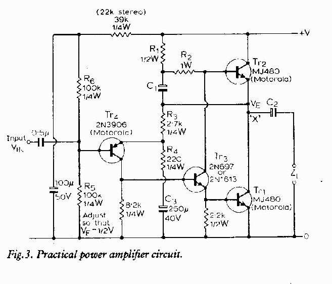
This schematic is a 10 watt amplifier for audio frequencies (approx. 50Hz-20kHz). The circuit is extremely simple, comprised of a total of only 18 components, 4 of which are transistors. Of the transistors used, 1 is a PNP (2N3906) , and 3 are NPN (2n697, 2 x NJ480).


Source : www.electrokits.com

Read More..

Sunday, December 22, 2013

Audio Amplifier Circuits 10W with Bass boost

Parts:
P1 22K Log.Potentiometer (Dual-gang for stereo)
P2 100K Log.Potentiometer (Dual-gang for stereo)
R1 820R 1/4W Resistor
R2,R4,R8 4K7 1/4W Resistors
R3 500R 1/2W Trimmer Cermet
R5 82K 1/4W Resistor
R6,R7 47K 1/4W Resistors
R9 10R 1/2W Resistor
R10 R22 4W Resistor (wirewound)
C1,C8 470nF 63V Polyester Capacitor
C2,C5 100uF 25V Electrolytic Capacitors
C3,C4 470uF 25V Electrolytic Capacitors
C6 47pF 63V Ceramic or Polystyrene Capacitor
C7 10nF 63V Polyester Capacitor
C9 100nF 63V Polyester Capacitor
D1 1N4148 75V 150mA Diode
IC1 NE5532 Low noise Dual Op-amp

Q1 BC547B 45V 100mA NPN Transistor
Q2 BC557B 45V 100mA PNP Transistor
Q3 TIP42A 60V 6A PNP Transistor
Q4 TIP41A 60V 6A NPN Transistor
J1 RCA audio input socket
Power supply parts:
R11 1K5 1/4W Resistor
C10,C11 4700uF 25V Electrolytic Capacitors
D2 100V 4A Diode bridge
D3 5mm. Red LED
T1 220V Primary, 12 + 12V Secondary 24-30VA Mains transformer
PL1 Male Mains plug
SW1 SPST Mains switch
Comments:
This design is based on the 18 Watt Audio Amplifier, and was developed mainly to satisfy the requests of correspondents unable to locate the TLE2141C chip. It uses the widespread NE5532 Dual IC but, obviously, its power output will be comprised in the 9.5 - 11.5W range, as the supply rails cannot exceed ±18V.
As amplifiers of this kind are frequently used to drive small loudspeaker cabinets, the bass frequency range is rather sacrificed. Therefore a bass-boost control was inserted in the feedback loop of the amplifier, in order to overcome this problem without quality losses. The bass lift curve can reach a maximum of +16.4dB @ 50Hz. In any case, even when the bass control is rotated fully counterclockwise, the amplifier frequency response shows a gentle raising curve: +0.8dB @ 400Hz, +4.7dB @ 100Hz and +6dB @ 50Hz (referred to 1KHz).
Notes:
Can be directly connected to CD players, tuners and tape recorders.
Schematic shows left channel only, but C3, C4, IC1 and the power supply are common to both channels.
Numbers in parentheses show IC1 right channel pin connections.
A log type for P2 ensures a more linear regulation of bass-boost.
Dont exceed 18 + 18V supply.
Q3 and Q4 must be mounted on heatsink.
D1 must be in thermal contact with Q1.
Quiescent current (best measured with an Avo-meter in series with Q3 Emitter) is not critical.
Set the volume control to the minimum and R3 to its minimum resistance.
Power-on the circuit and adjust R3 to read a current drawing of about 20 to 25mA.
Wait about 15 minutes, watch if the current is varying and readjust if necessary.
A correct grounding is very important to eliminate hum and ground loops. Connect in the same point the ground sides of J1, P1, C2, C3 &C4. Connect C9 at the output ground.
Then connect separately the input and output grounds at the power supply ground.
Technical data:
Output power: 10 Watt RMS @ 8 Ohm (1KHz sinewave)
Sensitivity: 115 to 180mV input for 10W output (depending on P2 control position)
Frequency response: See Comments above
Total harmonic distortion @ 1KHz: 0.1W 0.009% 1W 0.004% 10W 0.005%
Total harmonic distortion @ 100Hz: 0.1W 0.009% 1W 0.007% 10W 0.012%
Total harmonic distortion @10KHz: 0.1W 0.056% 1W 0.01% 10W 0.018%
Total harmonic distortion @ 100Hz and full boost: 1W 0.015% 10W 0.03%
Max. bass-boost referred to 1KHz: 400Hz = +5dB; 200Hz = +7.3dB; 100Hz = +12dB; 50Hz = +16.4dB; 30Hz = +13.3dB

Read More..

Saturday, December 21, 2013

TDA2006 12W Audio Amplifier Circuit

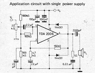
TDA2006 - 12W Audio Amplifier CircuitThis 12w amplifier circuit is build round the TDA2006 integrated circuit who options a brief circuit protection system, and a thermal shutdown system in case of overheating. With a 12v power supply the circuit delivers 12w on a 4 ohm speaker and 8w on a 8 ohm speaker. The integrated circuit will work with a power supplyr between 6v and 15v max.


The TDA2006 is monolithic integrated circuit in package, {supposed to be used as a low frequency category "AB" amplifier. At ±12V, d = 10 and frequently it provides 12W output power on a 4Ω load and 8W on a 8Ω . The TDA2006 provides high output current and has terribly low harmonic and cross-over distortion. any the device incorporates an inspired (and patented) short circuit protection system comprising a rendezvous for automatically limiting the dissipated power therefore on keep the operating urpose of the output transistors at intervals their safe operating space. a standard thermal shutdown system is additionally included. The TDA2006 is pin to pin equivalent to the TDA2030

Read More..

Wednesday, December 18, 2013

3 Channel Audio Mixer Circuit


Although the modular Portable Mixer architecture accessible on these web pages has become a hit for abounding amateurs, some correspondents appropriate a abundant simpler device, mainly for bond address signals.

This architecture should fulfil their needs, featuring three inputs with switchable high/low acuteness and abnormal level-control circuits, accouterment aerial afflict margins and low-noise figures, proportional to gain-level settings. Low accepted burning due to a simple, five-transistor circuitry, allows the Mini Mixer to be powered by a accepted 9V PP3 array for abounding hours.
Read More..

Tuesday, December 17, 2013

Low voltage audio amplifier circuit from 0 9 volts

Here i share power amplifier based on IC TDA7236 . This amplifier require minimum voltage 0,9 volt and maximum voltage is 1, 6 volt , its very low voltage amplifier. You can use this amplifier everywhere just with one battery 1,5 volt. Power output 16 mW with 32 ohms impedance. see circut below :
Read More..

LM3886 High Performance Audio Power Amplifier

LM3886 | High Performance Audio Power Amplifier
Audio Power Amplifier is an important part in sound reproduction ina sound system. Audio Power Amplifier with this power IC LM 3886Audio Power Amplifier is a highly capable and able to produce68 Watt power avg. 4Ohm load and capable of producing power 38 Watt8Ohm load.

With good sound reproduction capabilities of 20Hz-20kHz also possessed this LM3886 Audio Power Amplifier. Audio Power Amplifier LM3886 Speaker is equipped with protection that will protect the circuit output from over-voltage, under-voltage, over-loads, a short circuit power supply, thermal run-away and the temperature peak. Audio Power Amplifier LM3886 also equipped with noise reduction that can keep the audio system from noise well.

Schematic power amplifier with LM3886

Feature owned LM3886 Audio Power Amplifier

  • 68W cont. avg. output power into 4Ω at VCC = ± 28V
  • 38W cont. avg. output power into 8Ω at VCC = ± 28V
  • 50W cont. avg. output power into 8Ω at VCC = ± 35V
  • 135W instantaneous peak output power capability
  • Signal-to-Noise Ratio ≥ 92dB
  • An input mute function
  • Output protection from a short to ground or to the supplies via internal current limiting circuitry
  • Output over-voltage protection against transients from inductive loads
  • Supply under-voltage protection, not allowing internal biasing to occur Pls | VEE | + | VCC | ≤ 12V, Thus eliminating turn-on and turn-off transients
  • 11-lead TO-220 package
  • Wide supply range 20V - 94V


Application of Audio Power Amplifier LM3886

  • Stereo audio system
  • Active Speaker
  • High End Audio Power TV
  • Suround Power Amplifier
Read More..

Monday, December 16, 2013

Low power audio amplifier with IC TA7066P

The TA7066P is original monolithic Intregated Circuit Audio Power Amplifier. Package IC is SIP10-16 and manufactered by TOSHIBA.  The above sequence is a series of low-grade intregated circuit amplifier , which was very small output . But this amplifier is very high impedance power output. For more details , see description below.
Technical information :
Min. Voltage   : 8   Volts DC
Max. Voltage  : 25 Volts DC
Max. Power    : 0,3 Watts
Impedance      : 150 Ohms
Min. Currents : 2,8 mA
Read More..

Audio Amplifier Using TDA1519

This audio amplifier circuit is based on the TDA1519 amplifier ic which can be used in audio applications which don’t need high output power .The TDA1519 circuit can deliver 2x6 watts output power .

Audio Amplifier Circuit Using TDA1519

TDA1519 is an integrated class-B dual output amplifier in a 9-lead single in-line (SIL) plastic medium power package is primarily developed for car radio applications.This amplifier electronic circuit project needs to be powered from a 14.4 volt DC power supply
Read More..

Wednesday, December 11, 2013

Stereo TDA2822 audio power amplifier circuit

Stereo TDA2822 audio amplifier circuit
In this series I use IC tda2822M as the main amplifier, but if you want to use in addition to IC TDA2822M you can use ic I mentioned this is KA2209, NJM2073, U2822B, U2823B. Output is issued no more than 4W, which had low output. Supply voltage from 3 volts to 16 volts.


Below its schematics of TDA2822 stereo audio power amplifier

TDA2822 amplifier schematics

Part description
R1 = 4.7R
R2 = 4.7R
C1 = 1uF
C2 = 100uF
C3 = 100uF
C4 = 0.1uF
C5 = 470uF
C6 = 1uF
C7 = 100uF
C8 = 0.1uF
C9 = 470uF
ICs = KA2209 , NJM2073 , TDA2822 , U2822B , U2823B
Read More..

Saturday, December 7, 2013

Classical audio power amplifier with IT and OT transformer

The circuit is devote to the radio receiver in which sound ( the gear ) is weak. With the help of this tool , which initially sounds as if far to be clearly audible. Power amplifier does not require much  electrical current source , because all components are not up to over 1 Mega . But the result was incredible because it can enhance the power of  catching the wave signal.

Troubleshooting :
Wether transistors placement is correct ?
Placement Elco ?
Check are cable .

If all components have benn checked , and the damaged has been replaced . Then try , turn the potentiometer slowly and listen to how the sound output by the speaker.
Read More..

Monday, December 2, 2013

Stereo STK013 audio amplifier circuit

stk 013 amplifier
On the amplifier circuit using ic STK, the same as my previous posting. However, in the above circuit has 2 inputs and 2 outputs, or commonly called a stereo amplifier. This issue of power amplifier 2 x 18Watt and has impedance 8. To stress that it takes about 35-38Volt.
Component list :
Resistor
R1 =  390K
R2 = 390K
R3 = 220K
R4 = 220K
R5 = 220K
R6 = 220K
R7 = 100R
R8 = 1R
R9 = 9.1K
R10 = 9.1K
R11 = 1R
Capacitor
C1 = 10uF
C2 = 10uF
C3 = 0.47uF
C4 = 0.47uF
C5 = 220uF
C6 = 0.047uF
C7 = 4700uF
C8 = 100uF
C9 = 1000uF
C10 = 100uF
C11 = 4700uF
C12 = 470uF
C13 = 0.047uF
IC
U1 = STK013
Read More..