Showing posts with label ic. Show all posts
Showing posts with label ic. Show all posts
Friday, October 24, 2014
IC 555 Design Note
The popular Timer IC 555 is extensively used in short duration timing applications. IC 555 is a highly stable integrated circuit functioning as an accurate time delay generator and free running multivibrator. But one of the serious problem in 555 timer design is the false triggering of the circuit at power on or when voltage changes. The article describes how IC555 is designed perfectly to avoid false triggering.
555 IC pin functions
Pin1 Ground
Pin2 Trigger
Pin3 Output
Pin 4 Reset
Pin 5 Control voltage
Pin 6 Threshold
Pin 7 Discharge
Pin 8 Vcc
Functional aspects of pins
Trigger Pin 2
Usually pin2 of the IC is held high by a pull up resistor connected to Vcc. When a negative going pulse is applied to pin 2, the potential at pin 2 falls below 1/3 Vcc and the flip-flop switches on. This starts the timing cycle using the resistor and capacitor connected to pins 6 and 7.
Reset pin 4
Reset pin 4 can be controlled to reset the timing cycle. If pin 4 is grounded, IC will not be triggered. When pin4 becomes positive, IC becomes ready to start the timing cycle. Reset voltage is typically 0.7 volts and reset current 0.1 mA. In timer applications, reset pin should be connected to Vcc to get more than 0.7 volts.
Control Voltage pin 5
Pin5 can be used to control the working of IC by providing a DC voltage at pin5. This permits the control of the timing cycle manually or electronically. In monostable operation, the control pin5 is connected to ground through a 0.01 uF capacitor. This prevents the timing interval from being affected by AC or RF interference. In the Astable mode, by applying a variable DC voltage at pin 5 can change the output pulses to FM or PWM.
Threshold pin 6 and Discharge pin 7
These two inputs are used to connect the timing components- Resistor and Capacitor. The threshold comparator inside the IC is referenced at 2/3 Vcc and the trigger comparator is referenced at 1/3 Vcc. These two comparators control the internal Flip-Flop of the circuit to give High or Low output at pin 3.When a negative going pulse is applied to pin 2, the potential at pin2 drops below 1/3 Vcc and the trigger comparator switches on the Flip-Flop. This turns the output high. The timing comparator then charges through the timing resistor and the voltage in the timing capacitor increases to 2/3 Vcc.( The time delay depends on the value of the resistor and capacitor.
That is, higher values, higher time).When the voltage level in the capacitor increases above 2/3 Vcc, the threshold comparator resets the Flip-Flop and the output turns low. Capacitor then discharges through pin 7.Once triggered, the IC will not responds to further triggering until the timing cycle is completed. The time delay period is calculated using the formula T= 1.1 Ct Rt. Where Ct is the value of Capacitor in PF and Rt is the value of Resistor in Ohms. Time is in Seconds.
How to eliminate false triggering?
The circuit diagram shown below is the simple monostable using IC 555. To eliminate the false triggering resistor R1 and Capacitor C1 are connected to the reset pin 4 of the IC. So the reset pin is always high even if the supply voltage changes. Moreover capacitor C3 connected close to the Vcc pin 8 acts as a buffer to maintain stable supply voltage to pin 8. Using this design, it is easy to avoid false triggering to a certain extent.
555 IC pin functions
Pin1 Ground
Pin2 Trigger
Pin3 Output
Pin 4 Reset
Pin 5 Control voltage
Pin 6 Threshold
Pin 7 Discharge
Pin 8 Vcc
Functional aspects of pins
Trigger Pin 2
Usually pin2 of the IC is held high by a pull up resistor connected to Vcc. When a negative going pulse is applied to pin 2, the potential at pin 2 falls below 1/3 Vcc and the flip-flop switches on. This starts the timing cycle using the resistor and capacitor connected to pins 6 and 7.
Reset pin 4
Reset pin 4 can be controlled to reset the timing cycle. If pin 4 is grounded, IC will not be triggered. When pin4 becomes positive, IC becomes ready to start the timing cycle. Reset voltage is typically 0.7 volts and reset current 0.1 mA. In timer applications, reset pin should be connected to Vcc to get more than 0.7 volts.
Control Voltage pin 5
Pin5 can be used to control the working of IC by providing a DC voltage at pin5. This permits the control of the timing cycle manually or electronically. In monostable operation, the control pin5 is connected to ground through a 0.01 uF capacitor. This prevents the timing interval from being affected by AC or RF interference. In the Astable mode, by applying a variable DC voltage at pin 5 can change the output pulses to FM or PWM.
Threshold pin 6 and Discharge pin 7
These two inputs are used to connect the timing components- Resistor and Capacitor. The threshold comparator inside the IC is referenced at 2/3 Vcc and the trigger comparator is referenced at 1/3 Vcc. These two comparators control the internal Flip-Flop of the circuit to give High or Low output at pin 3.When a negative going pulse is applied to pin 2, the potential at pin2 drops below 1/3 Vcc and the trigger comparator switches on the Flip-Flop. This turns the output high. The timing comparator then charges through the timing resistor and the voltage in the timing capacitor increases to 2/3 Vcc.( The time delay depends on the value of the resistor and capacitor.
That is, higher values, higher time).When the voltage level in the capacitor increases above 2/3 Vcc, the threshold comparator resets the Flip-Flop and the output turns low. Capacitor then discharges through pin 7.Once triggered, the IC will not responds to further triggering until the timing cycle is completed. The time delay period is calculated using the formula T= 1.1 Ct Rt. Where Ct is the value of Capacitor in PF and Rt is the value of Resistor in Ohms. Time is in Seconds.
How to eliminate false triggering?
The circuit diagram shown below is the simple monostable using IC 555. To eliminate the false triggering resistor R1 and Capacitor C1 are connected to the reset pin 4 of the IC. So the reset pin is always high even if the supply voltage changes. Moreover capacitor C3 connected close to the Vcc pin 8 acts as a buffer to maintain stable supply voltage to pin 8. Using this design, it is easy to avoid false triggering to a certain extent.
555 Monostable circuit

A ready recknor to select timing resistor and capacitor

Theoretically long interval is possible with IC 555,but in practical conditions, it is difficult to get more than 3 minutes. If low leakage Tantalum capacitor is used, this can be increased to 5 minutes or more. If the value of the timing capacitor is too high above 470 uF, charging time will be prolonged which will upset the timing cycle and the output remains high even after the desired time is over.
http://www.extremecircuits.net

Thursday, February 27, 2014
Basic IC MonoStable Multivibrator

Basic LM555 Timer CIRCUIT
Part List
C2 = .01uf
IC1 = LM555 Timer
SWI = n.o. momentary switch
R1 and C1 determine lenght of
out put pulse where t = R1 x C1
and R1 is in ohms and C1 is in farads .
by Tony van Roon
Saturday, February 8, 2014
Schematic Power Amplifier with IC TDA7370
Here..... this circuit is stereo power amplifier , based on IC TDA7370, its nice Intregated Power amplifier , He does not have hre slightest sound buzzing , although power amplifiers without additional reinforcement , such as filters , tone control, etc.

Voltage : 9 to 24 volts
Max. Power Output : 2 x 20 Watts
Impedance : 4 Ohms
Friday, February 7, 2014
Small Power Amplifier with IC TDA1908
Schematic circuit power amplifier TDA1908 , or you can use IC TDA1908A . The circuit simple and easy to make the line PCB. See circuit and technical instruction below :

Minimum require voltage : 6 Volts
Maximum require coltage : 30 Volts
Maximum Power output : 16 Watts
Minimum Power output : 4 Watts
Read More..
The circuit above can use to the 5.1 surround sound circuit , but you have made 6 circuit and to combine to 1 . And suitable made to center speakers.Technical information :
Minimum require voltage : 6 Volts
Maximum require coltage : 30 Volts
Maximum Power output : 16 Watts
Minimum Power output : 4 Watts
Led Flasher with the LM3909 IC streampowers
The LM3909 is an integrated circuit (IC) which will flash a light-emitting diode (LED). Using only two extra components and a battery, the circuit is cheap and has a very low current drain from a 1.5 V cell.
The circuit can be used as a novelty flasher, an indicator for a dummy alarm bell box, or it could be attached to a torch so that it could be found easily in the dark! The simple circuit
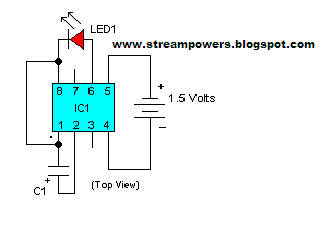
Led Flasher with the LM3909 IC Diagram
Assembly
The circuit can be built on a small piece of Veroboard (the piece shown in Figure 2 measures 15 holes by 10 strips). Using such a board, follow these instructions.
1. Depending on how far away you want the LED from the circuit board, solder a length of insulated wire to each lead of the LED. Use different colours of insulation – say, red and black, connecting the red lead to the anode (a) lead (the longer one) of the LED, and the black one to the cathode (k). Figure 2 shows these leads.
2. Cut the copper tracks as shown in Figure 2, using a 3 mm (1⁄8 inch) diameter drill, rotated between thumb and forefinger, or use the proper tool. Make absolutely sure that the tracks are completely broken!
3. Fit the IC holder in the correct position, using the cut tracks as guides, and make sure the small notch is facing towards the top of the board. Solder the pins to the copper tracks.
4. Mount the capacitor, positive end to the left, so that the positive lead is soldered to track F, which connects it to pin 2 of the IC; the negative lead is soldered to the right-hand side of track E, this being connected to pin 8 of the IC.
5. Solder on the battery leads, positive to the right, and the extended LED leads, positive downwards.
6. Check the circuit, and hold up the board to a bright light and look carefully for solder bridges between the tracks and pieces of copper swarf which may have escaped your inspection in 2 above! Remove whatever you find.
7. When all seems well, put the IC into the socket, ensuring that the notch or dot on the upper surface of the IC lines up with the notch on the holder. Line up each pin on the IC with the hole below it before pressing gently on the IC with the board supported on a firm surface.
8. Connect the battery; the LED should start to flash. The circuit is complete and working!
If you prefer, the whole circuit (battery included) can be mounted in a small plastic box, with the LED mounted on a clip and protruding through the panel. There are many other possibilities, and it is up to you to find an application for your own use.
Parts list
LM3909 Integrated circuit
IC socket 8-pin DIL BL17T
LED 5 mm diameter WL27E
100 microfarad (#F) Electrolytic capacitor (10 V) FB48C
Battery holder For AA-size cell YR59P
Battery 1.5 V AA cell
Small piece of Veroboard (15 holes by 10 strips)
Small plastic box (if required)
LED clip (if required)
Two lengths of coloured, insulated wire for LED (as required)
Sunday, January 26, 2014
Power amplifier circuit with IC LM386

IC LM386 is working for the amplifier audio circuit with a low power output , range from 0.325 watts to 2 watts with impedance 8 ohm. In this circuit requires voltage of 12 volts to the maximum work, and maximum current 3 Amp.Components List :R1=33K / 0,25WR2=1K / 0,25WR3=10R / 1WC1=100nC2=0,1uF/35VC3=100uF/16VC4=220uF/35VC5=4,7uF/16VIC1=LM386Connector Instruction:X-1 = Input , connect to outputX-2 = Input GroundX1-1= V+ , 12 Volt DCX1-2= V-/ GroundX1-3= Speaker+X1-4= Speaker-
Thursday, January 9, 2014
Low Power Audio Amplifier Circuit with IC TDA2824S
This is stereo audio amplifier with based on ICTDA2824S , Minimum voltage require 3 volts and maximum voltage 17 volts . Maximum output power 2 X 2 Watt , its low power amplifier. Output impedance 4 ohm. see schematic audio below :

Friday, December 27, 2013
Unique amplifier circuit schmeatic based on IC TDA7255
This circuit equipped with 2 switches that are useful for loudness and filtering, on SW1 as the loudness , SW2 as a filter. It also equipped with direct adjust of sound on Potentiometer 10k , but only useful as a master volume.

Minimum Voltage : 8 volts
Maximum Voltage : 18 volts
Maximum Power : 2 X 13 Watt stereo
Impedance Power : 4 Ohms
Monday, December 23, 2013
Multiplexer with CMOS IC 4556
In addition to the family of TTL ICs that support the function of a multiplexer is a family of CMOS ICs.

Read More..
Despite the fact it is the family of TTL ICs that support more functions than the CMOS multiplexer. For the working principle of the multiplexer IC CMOS family is actually tantamount to a multiplexer circuit, or IC TTL logic gates. That should be all referring to the real multiplexer function, namely the determination of output lines which represent the number of input lines. The use of symbols is possible between TTL and CMOS IC has a different but actually run the same rules. For your reference if you are interested in using family of CMOS IC 4556 series in particular, I include also the truth table below:
INPUT | OUTPUT | |||||
E | A0 | A1 | O0 | O1 | O2 | O3 |
L | L | L | L | H | H | H |
L | H | L | H | L | H | H |
L | L | H | H | H | L | H |
L | H | H | H | H | H | L |
H | X | X | H | H | H | H |
L = LOW | ||||||
H = HIGH | ||||||
Monday, December 16, 2013
Low power audio amplifier with IC TA7066P

The TA7066P is original monolithic Intregated Circuit Audio Power Amplifier. Package IC is SIP10-16 and manufactered by TOSHIBA. The above sequence is a series of low-grade intregated circuit amplifier , which was very small output . But this amplifier is very high impedance power output. For more details , see description below.
Technical information :Min. Voltage : 8 Volts DCMax. Voltage : 25 Volts DCMax. Power : 0,3 WattsImpedance : 150 OhmsMin. Currents : 2,8 mA
Schematic Power Amplifier with IC AN7116 Mono Amplifier
*notif : this is mono amplifier.
On this schematic circuit power amplifier with IC AN7116 , this schematic only use the IC because itsnot have similiar IC. To operate the Circuit , you must have any components too , such as resistor , condensator , etc. In order to be a circuit that works on good power amplifier.
This Circuit requires minimum voltage 3 volt and maximum voltage 9 volt . Ouput power of this circuit is 1 watt, and impedance is 4 Ohm.
To see Schematic Circuit ,please see below on figure 1.0 :
 | |||
| Figure 1.0 |
 |
| This package of IC : SIL-9 |
Sunday, December 15, 2013
Ramp Generator With 555 Timer IC
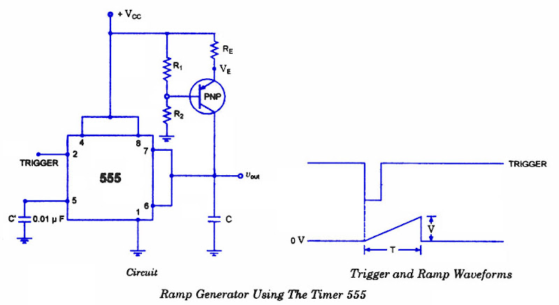 We apperceive that if a capacitor is answerable from a voltage antecedent through a resistor, an exponential waveform is produced while charging of a capacitor from a connected accepted antecedent produces a ramp. This is the abstraction abaft the circuit. The circuit of a access architect application timer 555 is apparent in figure. Here the resistor of previous circuits is replaced by a PNP transistor that produces a connected charging current.
Charging current produced by PNP constant current source is
iC = Vcc-VE / RE
where VE = R2 / (R1 + R2) * VCC + VBE
When a trigger starts the monostable multivibrator timer 555 as shown in figure, the PNP current source forces a constant charging into the capacitor C. The voltage across the capacitor is, therefore, a ramp as illustrated in the figure. The slope of the ramp is given as
Thursday, December 12, 2013
USB Charger Using IC MAX1555
This USB charger circuit is designed using the MAX1555 IC circuit manufactured by Maxim Semiconductor This MAX1555 USB charger can be used using the USB power or AC power.This MAX1555 charger is charging at 100mA from USB port and the maximum charging current increases to 350mA if the USB the AC adapter is connected . If both power types are connected in the same time the AC adapter is automatically given precedence.
USB Charger Circuit diagram
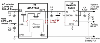
This charger can be used for small devices like : PDAs ,Cell Phones , Digital Cameras , MP3 Players and other.The charger can be used for Li-Ion or Li-Polymer batteries . The electronic project charger circuit require a input voltage between 3V and 7 V and deliver an 3.3 V output voltage.As you can see in the circuit diagram , before the IC is connected the MAX8881 linear regulator IC which is capable to deliver up to 200mA.The MAX1881 is specially designed for battery-powered applications where reverse battery protection and long battery life are critical.
USB Charger Circuit diagram
This charger can be used for small devices like : PDAs ,Cell Phones , Digital Cameras , MP3 Players and other.The charger can be used for Li-Ion or Li-Polymer batteries . The electronic project charger circuit require a input voltage between 3V and 7 V and deliver an 3.3 V output voltage.As you can see in the circuit diagram , before the IC is connected the MAX8881 linear regulator IC which is capable to deliver up to 200mA.The MAX1881 is specially designed for battery-powered applications where reverse battery protection and long battery life are critical.
Sunday, December 8, 2013
Schematic Power Amplifier with IC AN7112
Schematic Circuit use the IC AN7112 with minimum voltage 4 Volt and maximum voltage 14 Volt. Recomeneded voltage is 9 Volt. Maximum output power 0,5 watt. This is low output power or mini amplifier sound. Impedance Speaker 8 Ohm and frequncy 40 Hz - 18 kHz. IC AN7112 has similarities with IC KA2212 , LA4140 , TA7313AP . PAckage of this IC is SIL - 9 and Manufactered by MATSUSHITA.
See Schematic power amplifier (figure 1.1) and Package IC (figure 1.0) below :
 | ||
Figure 1.1 Click Image to View Enlarge
|
Monday, November 25, 2013
Schematic Audio Amplifier with IC AN313
This schematic very suitable applied on small speakers. Because the maximum output is 3W and the minimum voltage is 12 Volt , this will make speaker does not damage quickly. If you use speaker with impedance 8 Ohm , you must make parallel circuit speaker dont use series circuit.
See This Schematic and datasheet IC AN313 below :

Datasheet IC AN313
Vcc = 12-20 V
Pout = 2x3 W
RL = 8 Ohm
Ft = 40hz -18Khz
Icco = 40 mA
Package = TABS6-16
Manufactered = MATSUSHITA
Or you can call, Datasheetnya IC AN313
Sunday, November 24, 2013
Schematic Audio Amplifier with IC AN7102S
This Schematic use IC AN7102S , this is setereo amplifier and have output speaker 7,5 mW with impedance 32 Ohm . Supply need 1Volt to 3 Volt , wow this amplifier low voltage. You can use this amplifier on radio is use battery . With just one battery with voltage 1,5 Volt you can play this amplifier.
See this Schematic below :
 |
| Click to Enlarge |
Datasheet IC AN7102S
Vcc = 1-3 V
Pout = 2X 7,5 mW
RL = 32 Ohm
Ft = 20hz - 20Khz
Icco = 7 mA
Package = DIP-18
Manufactered = MATSUSHITA
Saturday, November 23, 2013
Schematic Audio Amplifier with IC AN5265
Schematic Description :
This Circuit Require voltage 12 -26 Volt. Good Voltage use is 16 Volt , Because its not too small and not too big Voltage. If use voltage that is to large it will quickly damage the IC. And if use voltage that is to small it will make less than maximum sound output.
See this Circuit and datsheet IC AN5265 Below :
 |
| Click to Enlarge |
Datasheet IC AN5265
Vcc = 12-26 V
Pout = 2,3 W
RL = 16 Ohm
Ft = 40hz - 18Khz
Icco = 9,5mA
Package = SIP2-9
Manufactered = MATSUSHITA
Vertical IC PIN OUT DATA
Vertical Vin = input (non-inverted), Vout = Vertical output, VfB = Vertical feedback (inverted inpput)
Vcc to pump-up can be traced through the diode PUM-up and pump up Elco Capacitor
VfB = or to Vin2
= Gnd or Vcc (-)
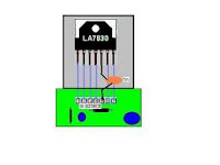
Vertical IC PIN-OUT DATA
AN5521 Vin = 4, Vout = 2, Vcc = 7, Gnd = 1, VfB =
AN5522 Vin = 7, Vout = 5, Vcc = 2, Gnd = 4, VfB = 1
AN5539 Vin = 4, Vout = 2, Vcc = 6, Gnd = 1, VfB = 5
AN15525 Vin = 7, Vout = 5, Vcc = 2, Gnd = 4, VfB = 1
LA7832 Vin = 4, Vout +2, Vcc = 6, Gnd = 1, VfB = 5
LA7835 = 2 Vin, Vout = 11, Vcc1 = 1, Vcc2 = 7,
LA7837 = 2 Vin, Vout = 12, Vcc1 = 1, Vcc2 = 8, Gnd = 11, VfB = 7
LA7838 = LA7837
LA7840 Vin = 4, Vout = 2, Vcc = 6, Gnd = 1, VfB = 5
LA7841 = LA7840
LA7845 = LA7840
LA7846 = 5 Vin, Vout = 3, Vcc = 7, Gnd = 2, VfB = 6
LA7848 Vina = 5, VinB = 6, Vout = 3, Vcc (+) = 7, Vcc (-) = 2
LA7876 Vina = 5, VinB = 6 Vcc (+) = 7, Vcc (-) = 2
STV9302 = see AN5522
STV9379 = See AN5522
TA8403 Vin = 4, Vout = 2, Vcc = 6, Vcc = 6,
TA8445 Vin = 2, Vout = 11, Vcc1 = 1 (9v), Vcc2 = 7 (26v), Gnd = 10, 50/60 =
TDA1771 Vin = 3, Vout = 1, Vcc = 9. Gnd = 5
TDA4865 Vin = 6, Vout = 5, Vcc = 1, Gnd = 4, VfB = 2
TDA8175 Vin = 7, Vout = 5, Vcc = 2, VfB = 1
TDA3653 Vin1 = 1, Vin2 = 3, Vcc1 = 9, Vcc2 = 6, Vou = 5, Gnd = 4
TDA8350 Vina = 1, VinB = 2, VoutA = 10, VoutB =, Vcc1 = 3, Vcc2 = 9, Ewin = 12, Ewout = 11
See tda8357 TDA8351 =
See TDA8357 TDA8356 =
TDA8357 Vina = 1, VinB = 2, VoutA = 7, VoutB = 4, Vcc1 = 3 (12v), Vcc2 = 6 (45V), Gnd = 5
TDA8358 Vina = 1, VinB = 2, Vcc1 = 3 (12v), Vcc2 = 9 (25V), VoutA = 4, VoutB = 10, Gnd = 6.7, Ewin = 5, Ewout = 8
TDA9302 = see LA78040
Read More..
Vcc to pump-up can be traced through the diode PUM-up and pump up Elco Capacitor
VfB = or to Vin2
= Gnd or Vcc (-)
Vertical IC PIN-OUT DATA
AN5521 Vin = 4, Vout = 2, Vcc = 7, Gnd = 1, VfB =
AN5522 Vin = 7, Vout = 5, Vcc = 2, Gnd = 4, VfB = 1
AN5539 Vin = 4, Vout = 2, Vcc = 6, Gnd = 1, VfB = 5
AN15525 Vin = 7, Vout = 5, Vcc = 2, Gnd = 4, VfB = 1
LA7832 Vin = 4, Vout +2, Vcc = 6, Gnd = 1, VfB = 5
LA7835 = 2 Vin, Vout = 11, Vcc1 = 1, Vcc2 = 7,
LA7837 = 2 Vin, Vout = 12, Vcc1 = 1, Vcc2 = 8, Gnd = 11, VfB = 7
LA7838 = LA7837
LA7840 Vin = 4, Vout = 2, Vcc = 6, Gnd = 1, VfB = 5
LA7841 = LA7840
LA7845 = LA7840
LA7846 = 5 Vin, Vout = 3, Vcc = 7, Gnd = 2, VfB = 6
LA7848 Vina = 5, VinB = 6, Vout = 3, Vcc (+) = 7, Vcc (-) = 2
LA7876 Vina = 5, VinB = 6 Vcc (+) = 7, Vcc (-) = 2
STV9302 = see AN5522
STV9379 = See AN5522
TA8403 Vin = 4, Vout = 2, Vcc = 6, Vcc = 6,
TA8445 Vin = 2, Vout = 11, Vcc1 = 1 (9v), Vcc2 = 7 (26v), Gnd = 10, 50/60 =
TDA1771 Vin = 3, Vout = 1, Vcc = 9. Gnd = 5
TDA4865 Vin = 6, Vout = 5, Vcc = 1, Gnd = 4, VfB = 2
TDA8175 Vin = 7, Vout = 5, Vcc = 2, VfB = 1
TDA3653 Vin1 = 1, Vin2 = 3, Vcc1 = 9, Vcc2 = 6, Vou = 5, Gnd = 4
TDA8350 Vina = 1, VinB = 2, VoutA = 10, VoutB =, Vcc1 = 3, Vcc2 = 9, Ewin = 12, Ewout = 11
See tda8357 TDA8351 =
See TDA8357 TDA8356 =
TDA8357 Vina = 1, VinB = 2, VoutA = 7, VoutB = 4, Vcc1 = 3 (12v), Vcc2 = 6 (45V), Gnd = 5
TDA8358 Vina = 1, VinB = 2, Vcc1 = 3 (12v), Vcc2 = 9 (25V), VoutA = 4, VoutB = 10, Gnd = 6.7, Ewin = 5, Ewout = 8
TDA9302 = see LA78040
Thursday, November 21, 2013
FM Moulator with IC 555
FM Modulator circuit is a simple FM modulation circuit using IC 555, where the resulting modulated signal has a tenuous meeting depends on the signal frequency information.

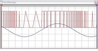
The resulting signal can be spelled out quite nice and stable so that the result will be more perfect. No winding or inductor in series modulator, so you do not need to bother to make a winding and calculate the value of the coil that you created it. With this circuit the desired value of frequency modulation can be obtained easily by calculating the frequency of IC 555 in general, which is determined by the resistor 6.8 K and 3.3 K and 0.1 UF capacitor. To obtain the other frequencies of your stay replace one or all three components.
Actually fm modulator ic 555 circuit is very simple though, but I think it reliable enough to handle a simple application purposes that do not require a big power or a very high frequency. But if you want more power you can add the RF amplifier circuit at the output of this circuit. Thus, the results of modulated signal can be amplified with the help of a series of supporters. In accordance with my experimental series modulators can work well at frequencies below the MHz range, because it is not IC IC 555 which is devoted to support of a very high frequency. You can use oscilltor transistor circuit, XTAL or others if you need a very high frequency.
The difference circuit with IC 555 on the multivibrator circuit in general is the use of pin 5, on the FM Modulator circuit is pin 5 of IC 555 is used as input information signal, which in turn will influence the shape of the output signal (modulated). But in applying this 5 pin multivibrator functions normally associated with 0.01 UF capacitor or left alone.
Subscribe to:
Posts (Atom)