Showing posts with label schematic. Show all posts

Friday, October 24, 2014

Low Cost Universal Battery Charger Schematic

Low cost solution for charging of both NiCd and NiMh batteries
Here is the circuit diagram of a low cost universal charger for NiCD - NiMH batteries. This circuit is Ideal for car use. It has ability to transform a mains adapter in to a charger . This one can be used to charge cellular phone, toys, portables, video batteries, MP3 players, ... and has selectable charge current. An LED is located in circuit to indicate charging. Can be built on a general purpose PCB or a veroboard. I hope you really like it.
Picture of the circuit:a_low_cost_universal_charger circuit schematic_for_nicd_nimh_batteries 
 A Low Cost Universal Charger Circuit Schematic
Circuit diagram:
a_low_cost_universal_charger_circuit_diagram_for_nicd nimh batteries
A Low Cost Universal Charger Circuit Diagram
Parts:
R1 = 120R-0...5W
R2 = See Diagram
C1 = 220uF-35V
D1 = 1N4007
D2 = 3mm. LED
Q1 = BD135
J1 = DC Input Socket
Specs:
  • Ideal for in car use.
  • LED charge indication.
  • Selectable charge current.
  • Charges Ni Cd or NiMH batteries.
  • Transforms a mains adapter into a charger.
  • Charge cellular phone, toys, portables, video batteries …
Features:
  • LED function indication.
  • Power supply polarity protected.
  • Supply current: same as charge current.
  • Supply voltage: from 6.5VDC to 21VDC (depending on used battery)
  • Charge current (±20%): 50mA, 100mA, 200mA, 300mA, 400mA. (selectable)
Determining the supply voltage:
This table indicates the minimum and maximum voltages to supply the charger. See supply voltage selection chart below.
Example:
To charge a 6V battery a minimum supply voltage of 12V is needed, the maximum voltage is then 15V.
Voltage selection:

supply_voltages_selection_chart_for_ ow cost universal_battery Charger
Voltage Selection Chart For Low Cost Universal Battery Charger

Determining the charge current:
Before building the circuit, you must determinate how much current will be used to charge the battery or battery pack. It is advisable to charge the battery with a current that is 10 times smaller then the battery capacity, and to charge it for about 15 hours. If you double the charge current , then you can charge the battery in half the time. Charge current selection chart is located in diagram.

Example:
A battery pack of 6V / 1000mAh can be charged with 100mA during 15 hours. If you want to charge faster, then a charge current of 200mA can be used for about 7 hours.
Caution:
The higher charge current, the more critical the charge time must be checked. When faster charging is used, it is advisable to discharge the battery completely before charging. Using a charge current of 1/10 of the capacity will expand the lifetime of the battery. The charge time can easily be doubled without damaging the battery.
Note:
  • Mount the transistor together with the heatsink on the PCB, bend the leads as necessary. Take care that the metal back of the transistor touches the heatsink. Check that the leads of the transistor do not touch the heatsink.
Source : http://www.ecircuitslab.com
Read More..

Simple Water Level Indicator Circuit Schematic

The whole project was developed on a friends request. Its purpose was to remotely monitor the water-level in a metal tank located in the attic by means of a very simple control unit placed in the kitchen, some floors below.
Mains requirements were:
  1. No separate supply for the remote circuit
  2. Main and remote units connected by a thin two-wire cable
  3. Simple LED display for the main unit
  4. Battery operation to avoid problems related to mains supply and water proximity
  5. As the circuit was battery operated a low current consumption was obviously welcomed
The very small remote unit is placed near the tank and measures the water level in three ranges by means of two steel rods. Each range will cover one third of the tank capacity:

Almost empty - signaled by means of a red LED (D3) in the control unit display
About half-level - signaled by means of a yellow LED (D2) in the control unit display
Almost full - signaled by means of a green LED (D1) in the control unit display

Circuit diagram:

Water-level Indicator Circuit Diagram

Circuit operation:

When the water-level is below the steel rods, no contact is occurring from the metal can and the rods, which are supported by a small insulated (wooden) board. The small circuit built around IC1 draws no current and therefore no voltage drop is generated across R5. IC2A, IC2B and Q1 are wired as a window comparator and, as there is zero voltage at input pins #2 and #5, D3 will illuminate. When the water comes in contact with the first rod, pin #13 of IC1 will go high, as its input pins #9 to #12 were shorted to negative by means of the water contact.

Therefore, R4 will be connected across the full supply voltage and the remote circuit will draw a current of about 9mA. This current will cause a voltage drop of about 0.9V across R5 and the window comparator will detect this voltage and will change its state, switching off D3 and illuminating D2. When the water will reach the second rod, also pin #1 of IC1 will go high for the same reason explained above. Now either R3 and R4 will be connected across the full supply voltage and the total current drawing of the remote circuit will be about 18mA.

The voltage drop across R5 will be now about 1.8V and the window comparator will switch off D2 and will drive D1. The battery will last very long because the circuit will be mostly in the off state. Current is needed only for a few seconds when P1 is pushed to check the water-level and one of the LEDs illuminates.

Parts:

R1 = 15K 1/4W Resistors
R2 = 15K 1/4W Resistors
R3 = 1K 1/4W Resistors
R4 = 1K 1/4W Resistors
R5 = 100R 1/4W Resistor
R6 = 47K 1/4W Resistor
R7 = 3.3K 1/4W Resistors
R8 = 3.3K 1/4W Resistors
R9 = 2.7K 1/4W Resistors
R10 = 15K 1/4W Resistors
R12 = 15K 1/4W Resistors
R13 = 3.3K 1/4W Resistors
R14 = 2.7K 1/4W Resistors
R15 = 2.7K 1/4W Resistors
D1 = 3mm Green LED
D2 = 3mm Yellow LED
D3 = 3mm Red LED
C1 = 470nF 63V Polyester or Ceramic Capacitor
J1 = Two ways output sockets
J2 = Two ways output sockets
P1 = SPST pushbutton
B1 = 9V PP3 Battery
Q1 = BC547 45V 100mA NPN Transistor
IC1 = 4012 Dual 4 input NAND gate IC
IC2 = LM393 Dual Comparator IC
Two steel rods of appropriate length
Read More..

Sunday, February 9, 2014

Low ripple power supply schematic

Simple schematic above is a circuit of power supply that can operate at high current with very small ripple voltage. How it works similiar to the high power class AB amplifiers, with the same quality. T1,T2 ,and R2 can also be called a power NPN-Darlington transistor. ZD1 and R1 as a supplier of voltage on the transistor base and filtered by C2. ZD1 can be slected with formulated (Figure 1.0) . For the C2 can be selected in accordance with the degree of smoothness as its value is effectively combined with the multiplied gain of the Transistor T1 and T2, assumsing minimum hfe for T1 and T2 , C=100x15(T1) x 25 (T2) = 37,000uF, adjust the voltage C2 with the input voltage, but must be higher than input voltage.
Low ripple power suplly regulator
Part List :
R1 = 2K2
R2 = 56R
R3 = 10K
C1 = 1500uF
D1-D4 = Didode 6A
T1 = 2N3054
T2 = 2N3055
rumus tegangan ripple
Figure 1.0
Read More..

Saturday, February 8, 2014

4 Transistor Transmitter Schematic

This circuit provides an FM modulated signal with an output power of around 500mW. The input Mic preamp is built around a couple of 2N3904 transistors, audio gain limited by the 5k preset. The oscillator is a colpitts stage, frequency of oscillation governed by the tank circuit made from two 5pF capacitors and the inductor. ( Click here for Colpitt Oscillator Resonant Frequency Equation.) Frequency is around 100Mhz with values shown.

4 Transistor Transmitter Circuit Diagram


Audio modulation is fed into the tank circuit via the 5p capacitor, the 10k resistor and 1N4002 controlling the amount of modulation. The oscillator output is fed into the 3.9uH inductor which will have a high impedance at RF frequencies.

The output stage operates as a class D amplifier, no direct bias is applied but the RF signal developed across the 3.9uH inductor is sufficient to drive this stage. The emitter resistor and 1k base resistor prevent instability and thermal runaway in this stage.
Read More..

Schematic Power Amplifier with IC TDA7370

Here..... this circuit is stereo power amplifier , based on IC TDA7370, its nice Intregated Power amplifier , He does not have hre slightest sound buzzing , although power amplifiers without additional reinforcement , such as filters , tone control, etc.
Voltage                      : 9 to 24 volts
Max. Power Output  : 2 x 20 Watts
Impedance                : 4 Ohms
Read More..

5 1 surround amplifier circuit schematic

This 5.1 surround amplifier circuit schematic use the IC AN7168 as the main component from this circuit . Minimum voltage required 12V and maximum voltage 24V , I recomended it 12 V because the voltage support on are components. But if you want to better a loud sound you can raise it. 

Maximum power output 40W with impedance 4 ohm . This 5.1 surround amplifier circuit schematic also support to make surround sound or 5.1 speaker. Use this amplifier on rear speaker , left right , and center but dont use to subwoofer speaker. See 5.1 surround amplifier circuit schematic below :

Click to view large
If you want to make a 5.1 surround sound you must make 5 the circuit of 5.1 surround amplifier circuit schematic , for left and right speaker , rear left and right speaker , and center speaker. Use the subwoofer speaker with support amlplifier subwoofer circuit .


Read More..

Tuesday, February 4, 2014

18W Amplifier Schematic Circuit

18W Amplifier Schematic Circuit

18W Amplifier Schematic Circuit Part List

P1_____________22K Log. Potentiometer (Dual-gang for stereo)

R1______________1K 1/4W Resistor

R2______________4K7 1/4W Resistor

R3____________100R 1/4W Resistor

R4______________4K7 1/4W Resistor

R5_____________82K 1/4W Resistor

R6_____________10R 1/2W Resistor

R7_______________R22 4W Resistor (wirewound)

R8______________1K 1/2W Trimmer Cermet (optional)

C1____________470nF 63V Polyester Capacitor

C2,C5_________100µF 3V Tantalum bead Capacitors

C3,C4_________470µF 25V Electrolytic Capacitors

C6____________100nF 63V Polyester Capacitor

D1___________1N4148 75V 150mA Diode

IC1________TLE2141C Low noise, high voltage, high slew-rate Op-amp

Q1____________BC182 50V 100mA NPN Transistor

Q2____________BC212 50V 100mA PNP Transistor

Q3___________TIP42A 60V 6A PNP Transistor

Q4___________TIP41A 60V 6A NPN Transistor

J1______________RCA audio input socket

Power supply parts:

R9______________2K2 1/4W Resistor

C7,C8________4700µF 25V Electrolytic Capacitors

D2_____________100V 4A Diode bridge

D3_____________5mm. Red LED

T1_____________220V Primary, 15 + 15V Secondary, 50VA Mains transformer

PL1____________Male Mains plug

SW1____________SPST Mains switch
Read More..

Monday, December 23, 2013

2 Transistor Transmitter Schematic

A compact 2 transistor transmitter for use at VHF frequencies.

2 Transistor Transmitter Schematic Circuit Diagram


Notes:
Transistor T1 works as an audio preamplifier, gain is fixed at approximately R2/R1 or 100 times. The audio input is applied at the points LF in (on the diagram). P1 works as gain control. After amplification this audio signal now modulates the transmitter built around T2. Frequency is tunable using the trimmer CT and L1 is made using 3 turns of 1mm copper wire wound on a 5mm slug. The modulated signal passes via C6 to the antenna. A dipole can be made using 2 lengths of 65cm copper pipe. A DC power supply in the range 3 to 16 volts is required.
Read More..

Thursday, December 19, 2013

70W STK amplifier schematic

home amplifier schematics
For this amplifier circuit using three voltage plus, min, and the ground. with a maximum voltage approximately 55Volt DC. And amplifier circuit can use some ic ie IC STK 030, 058, 075, 077, 078, 080, 082, 083, 084, 086. From all the ic I mentioned all of them can be applied to this amplifier circuit. But every ic whether there might be a different maximum voltage or power output, etc.. For this amplifier suitable for use at home, who need a voice soft and tasty. With a maximum output of 70W 8ohm impedance is my take of the highest IC output is STK086.
Part List
R1 = 1K
R2 = 56K
R3 = 100R
R4 = 100R
R5 = 56K
R6 = 4.7R
R7 = 2.7K
C1 = 1uF
C2 = 470pF
C3 = 100uF
C4 = 100uF
C5 = 0.047uF
C6 = 47uF
C7 = 1800pF
C8 = 10uF
IC = STK 030, 058, 075, 077, 078, 080, 082, 083, 084, 086.
Read More..

Monday, December 16, 2013

Schematic Power Amplifier with IC AN7116 Mono Amplifier

*notif :  this is mono amplifier.

   On this schematic circuit power amplifier with IC AN7116 , this schematic only use the IC because itsnot have similiar IC. To operate the Circuit , you must have any components too , such as resistor , condensator , etc. In order to be a circuit that works on good power amplifier.
  This Circuit requires minimum voltage 3 volt and maximum voltage 9 volt . Ouput power of this circuit is 1 watt, and impedance is 4 Ohm.

To see Schematic Circuit ,please see below on  figure 1.0 :


Figure 1.0


And see Package IC AN7116 below :

This package of IC : SIL-9
Read More..

Sunday, December 15, 2013

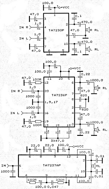
TA7230P TA7236P TA7237AP amplifier schematic

Amplifier circuit here is all based on the ic in the gains. Three IC TA7230P, TA7236P, TA7237AP is intregated circuit (IC) which was applied to the power amplifier. Each IC has a different output, different input voltage, all IC TA7230P, TA7236P, TA7237AP is manufactured by Toshiba.

You can see maximum minimum voltage , power output , and other here
TA7230P, TA7236P, TA7237AP amplifier schematic
Read More..

Sunday, December 8, 2013

Schematic Power Amplifier with IC AN7112

Schematic Circuit use the IC AN7112 with minimum voltage 4 Volt and maximum voltage 14 Volt. Recomeneded voltage is 9 Volt. Maximum output power  0,5 watt. This is low output power or mini amplifier sound. Impedance Speaker 8 Ohm and frequncy 40 Hz - 18 kHz. IC AN7112 has similarities with IC KA2212 , LA4140 , TA7313AP . PAckage of this IC is SIL - 9 and Manufactered by MATSUSHITA.

See Schematic power amplifier (figure 1.1) and Package IC (figure 1.0)  below :

Figure 1.1 Click Image to View Enlarge
Figure 1.0
Read More..

Saturday, December 7, 2013

Glitch Detector Schematic

In the circuit, two op amps (half of an LM324 quad op amp) and an SCR are direct coupled in a de-voltage monitoring circuit. Op-amp U1-a is configured as a voltage follower, which feeds the bridged inputs of the second op amp, Ul-b. A resistor/capacitor combination (R2/C1) connected to the negative input of U1-b forms an RC time-delay circuit.

Glitch Detector Circuit Schematic


As long as there is no change in the de-voltage level at either of U1-bs inputs, its output is near zero. If a voltage glitch occurs, the RC timing circuit will delay the voltage change at the op amps inverting input, causing its output to go high, triggering SCR1 and causing LED1 to light. The circuits sensitivity allows it to detect voltage changes in the millivolt range. Pressing S1 diverts the SCRs holding current to ground, causing it to turn off and reset the circuit.
Read More..

Tuesday, November 26, 2013

50W car audio amplifier schematic circuits

50W car amplifier schematicsCar power amplifier uses SI1050GL IC as the main amplifier. The output power 50 Watt 8 ohm mono impedance. Up to 25 Volt DC voltage. with source voltage of this amplifier car battery has to work.


Minimum of 12 Volt battery voltage, less than a sound or audio is issued less than the maximum and less good. You can assemble  this circuit amplifier with a schema like this.
50W car amplifier system
Part List
R1 = 100K
R2 = 1R
C1 = 2.2uF
C2 = 22uF
C3 = 100uF
C4 = 0.1uF
C5 = 100uF
U1 = SI1050GL
If you want to make stereo amplifier , you must required multiply the two of components. 


Read More..

Monday, November 25, 2013

Schematic Audio Amplifier with IC AN313

This schematic very suitable applied on small speakers. Because the maximum output is 3W and the minimum voltage is 12 Volt  , this will make speaker does not damage quickly. If you use speaker with impedance 8 Ohm , you must make parallel circuit speaker dont use series circuit.
See This Schematic and datasheet IC AN313 below :


Datasheet IC AN313
Vcc                = 12-20 V
Pout               =  2x3 W
RL                  = 8 Ohm
Ft                   = 40hz -18Khz
Icco                = 40 mA
Package         = TABS6-16
Manufactered = MATSUSHITA
Or you can call, Datasheetnya IC AN313
Read More..

Sunday, November 24, 2013

Schematic Audio Amplifier with IC AN7102S

This Schematic use IC AN7102S , this is setereo amplifier and have output speaker 7,5 mW with impedance 32 Ohm . Supply need 1Volt to 3 Volt , wow this amplifier low voltage. You can use this amplifier on radio is use battery . With just one battery with voltage 1,5 Volt you can play this amplifier.
See this Schematic below :


Click to Enlarge


Datasheet IC AN7102S
Vcc                   =  1-3 V
Pout                 = 2X 7,5 mW
RL                    = 32 Ohm
Ft                      = 20hz - 20Khz
Icco                  = 7 mA
Package         = DIP-18
Manufactered = MATSUSHITA
Read More..

Saturday, November 23, 2013

Schematic Audio Amplifier with IC AN5265

Schematic Description :
This Circuit Require voltage 12 -26 Volt. Good Voltage use is 16 Volt , Because its not too small and not too big Voltage. If use voltage that is to large it will quickly damage the IC. And if use voltage that is to small it will make less than maximum sound output.
See this Circuit  and datsheet IC AN5265 Below :

Click to Enlarge

Datasheet IC  AN5265
Vcc                = 12-26 V
Pout               = 2,3 W
RL                  = 16 Ohm
Ft                   = 40hz - 18Khz
Icco                = 9,5mA
Package         = SIP2-9
Manufactered =  MATSUSHITA
Read More..