Showing posts with label power. Show all posts

Friday, October 24, 2014

8 Amp Regulated Power Supply circuit Diagram

This power supply is powered by a transformer operating from 120 Vac on the primary and providing proximately 20 Vac on the primary, and providing approximately 20 Vac on the secondary. Four 10-A diodes with a 100 PIV rating are used in a full-wave bridge rectifier.

 8-Amp Regulated Power Supply Circuit Diagram


8-Amp Regulated Power Supply circuit Diagram

A 10,000 ^F/36 Vdc capacitor completes the filtering, providing 28 Vdc. The dc voltage is fed to the collectors of the Darlington connected 2N3055s. Base drive for the pass transistors is from pin 10 of the µ723 through a 200 ohm current limiting resistor, Rl. The reference terminal (pin 6) is tied directly to the non-inverting input of the error amplifier (pin 5), providing 7.15 V for comparison. Link

The inverting input to the error amplifier (pin 4) is fed from the center arm of a 10 k ohm potentiometer connected across the output of the supply. This control is set for the desired output voltage of 13.8 V. Compensation of the error amplifier is accomplished with a 500 pF capacitor connected from pin 13 to pin 4. If the power supply should exceed 8 A or develop a short circuit, the µ723 regulator will bias the transistors to cutoff and the output voltage will drop to near zero until the short circuit condition is corrected.
Read More..

Monday, October 20, 2014

High LASER Power Supply

If you have ever worked with lasers, you know how fun and interesting it can be, you also know how expensive it can be. The high voltage power supplies for the laser tubes are often more expensive then the tubes themselves. This supply can be built with commmon parts, most of which you probably already have in your junk box. The secret is the transformer used. It is a common 9V 1A unit, connected backwards for step up. 
 
Please note that some people may have trouble with this supply. This is due to the slight difference in transformers.

CAUTION:LASER RADIATION

Schematic


This is the schematic of the laser power supply

Parts


Part

Total Qty.

Description

Substitutions
R1
1
10 Ohm 10W Or Greater Resistor
R2
1
Ballast Resistor, See "Notes"
D1, D2, D3
3
1N4007 Silicon Diode
C1, C2, C3
3
0.1 uF 2000V Capacitor
T1
1
9V 1A Transformer
S1
1
115V 2A SPST Switch
MISC
1
Case, Wire, Binding Posts (for output), Line Cord

Notes

1. T1 is an ordinary 9V 1A transformer connected backwards for step up.
2. R1 MUST be installed on a LARGE heatsink. A good heatsink is the metal case the supply is built in.
3. R2 Protects the laser tube from excess current. It should be soldered directly to the anode terminal on the tube. To find R2, start with a 500K 10W resistor and work down until the tube lights and remains stable.
4. If you have trouble with the tube not starting easily, use a longer anode lead that is wrapped around the tube.
5. Depending on the transformer you use, the circuit may or may not work. I cannot guarantee the operation of this circuit. Build at your own risk.
Read More..

Now 0 to 40V Lab Power Supply

A very lab adjustable power supply that can provide an output voltage between 0 and 60 volts can be designed using this circuit diagram . This lab power supply can be designed with LM723 chip or for higher output voltages, with L146 .Output current is also adjustable, but once established, is always effective. Table 1 shows the values to be modified to have three different versions of the maximum output voltage (30, 40 and 60 V).


Electrical diagram below shows the alternative 40 V / 0.8 using L146 chip because it can stabilize higher output voltage, much better than the LM723. Normally, 2 V is the minimum voltage stabilized that even an integrated circuit can provide. Resistive network R3, R4 and R5, R6 "kill" this restriction so that output can be set to 0 V with potentiometer P2.

0 to 40V Lab Power Supply

Depending on the output requirements, will be decided on the type and the semiconductor capacitors to be used. Output current must be limited so as to keep power dissipation of 40 W. T3 under maximum output current for 40 V version is 0.8 A. It can connect two parallel 2N3055 transistors (with emitter resistors) to double the current output, but in this case requires a 2 A transformer
Read More..

Saturday, October 11, 2014

Low Power Voltage Doubler Circuit Diagram

All miniature electronic devices operate off batteries. Some of them need higher than the standard battery voltages to operate efficiently. If the battery of that specific voltage is unavailable, we are forced to connect additional cells in series to step up the DC voltage. Thus, the true meaning of miniaturisation is lost. A simple way to overcome this problem is to employ a voltage doubler, if the device under consideration can operate at a small current.

Here we present a low-power voltage doubler circuit that can be readily used with devices that demand higher voltage than that of a standard battery but low operating current to work with. The circuit is quite simple as it uses only a few components. Yet, the output efficiency is 75 to 85 percent along its operating voltage range. The available battery voltage is almost doubled at the output of the circuit.

Here IC1 is wired as an astable multivibrator to generate rectangular pulses at around 10 kHz. This frequency and duty cycle of the pulses can be varied using preset VR1. The pulses are applied to switching transistors T1 and T2 for driving the output section, which is configured as a voltage-doubling circuit. The doubled voltage is available across capacitor C5. During each cycle of the pulse occurance, the high level drives T1 into its saturation, keeping transistor T2 cut off.

Circuit diagram:

Low-Power Voltage Doubler Circuit Diagram

So transistor T1 charges capacitor C4 via the path formed by diodes D2 and D1 to a voltage level slightly lesser than the supply. But during the low period of the pulse, transistor T1 is cut off while transistor T2 is driven into saturation. Now, transistor T2 raises the charge on the negative pole of capacitor C4 by another step equal to the supply voltage. Therefore an equal amount of charging is built up on capacitor C5 via diode D3.

This doubling action increases the total voltage across capacitor C5 to almost double the input voltage. If the output of the pulse generator is maintained with a high enough amplitude and frequency, the output voltage and current remain constant and cater to the needs of the load. Even with the half-wave function, this circuit is almost free of ripple voltage. If the connected load doesn’t require a high current, the efficiency can be expected in the upper 90 percentranges.

Since the input voltage is doubled, the current drain from the input power supply is also doubled at the input but halved at the output. One point of caution is that if the multivibrator’s frequency is fairly high, the output may suffer with the interference imposed over the DC voltage. In this case, the frequency must be set favorably by trials and actual load connection procedure. This tiny circuit can be assembled on the general-purpose PCB. If all of the components are surface-mount type, the whole module can be genuinely miniaturized.

EFY Lab note. During testing with input of 8V and 1.25mA load current the output voltage was found to be around 13V.

Author :M.K. Chandra ,Mouleeswaran And A.N. Vadivudai Naayaki
 
 
Source
: www . efymag . com
Read More..

Build a 1 2 36V 5A Adjustable Power Supply with LM317

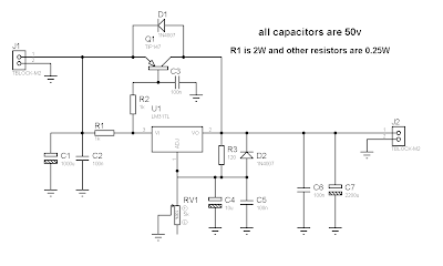
Build a 1.2-36V 5A Adjustable Power Supply circuit diagram with LM317. This circuit is a simple power supply circuit. 1.2 - 36V adjustable bench power supply with 5A of output current. Max input voltage is 37V and output is adjustable via potentiometer between 1.2 up to 36 volts. TIP147 PNP darlington transistor boosts the current of LM317 from 100mA to 5A. LM317 is the most useful and inexpensive adjustable regulator and for this circuit you can also use LM317 L that can give 100mA, thats enough for transistor bias. 

 1.2-36V 5A Adjustable Power Supply Circuit Diagram

1.2-36V 5A Adjustable Power Supply with LM317

 D1 and D2 are protection diodes because when you turn the circuit off the output capacitors are discharging and can damage the transistor or regulator. 100nf capacitors are in parallel with electrolytic capacitors to remove high frequency noise because large value electrolytic have large ESR and ESL and cant remove high frequency noise.
Read More..

How to Repairing Switching Power Supply

Up to date power supply are renowned as "switching controller power supply." In most swapping supply, the 110 volt AC input is first rectified by two diodes and filtered by a pair of capacitors. This conceives two high- voltage causes; one positive and the other negative. A pair of transistors is then utilized to switch these high voltage supply over the primary winding of a transformer. 

This switching activity is very fast. A usual switching pace is around 40,000 circuits per second or 40KHz. An integrated circuit is commonly utilised to control the transistors. This IC not only controls the pace at which the transistors are swapped, but furthermore controls the amount of time that each transistor is energized. The yield voltage of the power supply is very resolute by the "on" time of the transistors. If the transistors are hold on for a longer time span of time, the output voltage of the provide will rise, while shorter times smaller the yield voltage. This is renowned as "pulse-width modulation." 

 Power Supply

How to  Repairing Switching Power Supply

Read More..

Thursday, September 18, 2014

Very Low Power 32kHz Oscillator

The 32-kHz low-power clock oscillator offers numerous advantages over conventional oscillator circuits based on a CMOS inverter. Such inverter circuits present problems, for example, supply currents fluctuate widely over a 3V to 6V supply range, while current consumption below 250 µA is difficult to attain. Also, operation can be unreliable with wide variations in the supply voltage and the inverter’s input characteristics are subject to wide tolerances and differences among manufacturers. The circuit shown here solves the above problems. Drawing just 13 µA from a 3V supply, it consists of a one-transistor amplifier/oscillator (T1) and a low-power comparator/reference device (IC1).

Circuit diagram:
very-low-power-32khz-oscillator-circuit-diagram Very Low Power 32kHz Oscillator Circuit Diagram

The base of T1 is biased at 1.25 V using R5/R4 and the reference in IC1. T1 may be any small-signal transistor with a decent beta of 100 or so at 5 µA (defined here by R3, fixing the collector voltage at about 1 V below Vcc). The amplifier’s nominal gain is approximately 2 V/V. The quartz crystal combined with load capacitors C1 and C3 forms a feedback path around T1, whose 180 degrees of phase shift causes the oscillation. The bias voltage of 1.25 V for the comparator inside the MAX931 is defined by the reference via R2. The comparator’s input swing is thus accurately centred around the reference voltage.

Operating at 3 V and 32 kHz, IC1 draws just 7 µA. The comparator output can source and sink 40 mA and 5 mA respectively, which is ample for most low-power loads. However, the moderate rise/fall times of 500 ns and 100 ns respectively can cause standard, high-speed CMOS logic to draw higher than usual switching currents. The optional 74HC14 Schmitt trigger shown at the circuit output can handle the comparator’s rise/fall times with only a small penalty in supply current.

Author: http://www.ecircuitslab.com/2011/06/very-low-power-32khz-oscillator.html
Read More..

Sunday, February 9, 2014

Low ripple power supply schematic

Simple schematic above is a circuit of power supply that can operate at high current with very small ripple voltage. How it works similiar to the high power class AB amplifiers, with the same quality. T1,T2 ,and R2 can also be called a power NPN-Darlington transistor. ZD1 and R1 as a supplier of voltage on the transistor base and filtered by C2. ZD1 can be slected with formulated (Figure 1.0) . For the C2 can be selected in accordance with the degree of smoothness as its value is effectively combined with the multiplied gain of the Transistor T1 and T2, assumsing minimum hfe for T1 and T2 , C=100x15(T1) x 25 (T2) = 37,000uF, adjust the voltage C2 with the input voltage, but must be higher than input voltage.
Low ripple power suplly regulator
Part List :
R1 = 2K2
R2 = 56R
R3 = 10K
C1 = 1500uF
D1-D4 = Didode 6A
T1 = 2N3054
T2 = 2N3055
rumus tegangan ripple
Figure 1.0
Read More..

10 Watt Power Amplifier Circuit

IC BA514 its the main of  this circuit. This is actually low power output with minimum power output 2 W but maximum output 10W . Minimum voltage require 9 Volt and maximum voltage 14 Volt . Impedance output 4 Ohm.
Power Amplifier Schematic below :


Click to view Larger
All capacitor with uF and minimum voltage capacitor is 16 V. resistor with 1/4 Watt.
Read More..

Power Supply with principle of UPS

power supply voltage
For UPS Power Supply circuit consists of lowering the voltage, rectifier, charger, batery and regulators. The technique is applied from UPS on the power supply is the use of batery and charger is connected dengang direct coupling with a series diode. For more details can be seen with the following image.

Ups power supply schematics
Schematics
The rectifier in the circuit UPS Power Supply For this to function also as a charger via D1. D3 function is to drain-source voltage of the rectifier to the regulator circuit, when the AC voltage source. D2 serves to drain the batery when the source voltage from AC voltage source does not exist. batery configuration and diode D1, D2 and D3 is adopted from the UPS system. may be useful and can provide inspiration on teman2 all in making backups on the system power supply voltage.
Read More..

Saturday, February 8, 2014

Schematic Power Amplifier with IC TDA7370

Here..... this circuit is stereo power amplifier , based on IC TDA7370, its nice Intregated Power amplifier , He does not have hre slightest sound buzzing , although power amplifiers without additional reinforcement , such as filters , tone control, etc.
Voltage                      : 9 to 24 volts
Max. Power Output  : 2 x 20 Watts
Impedance                : 4 Ohms
Read More..

Friday, February 7, 2014

Small Power Amplifier with IC TDA1908

Schematic circuit power amplifier TDA1908 , or you can use IC TDA1908A . The circuit simple and easy to make the line PCB. See circuit and technical instruction below : 

The circuit above can use to the 5.1 surround sound circuit , but you have made 6 circuit and to combine to 1 .  And suitable made to center speakers.
Technical information :
Minimum require voltage :  6 Volts
Maximum require coltage :  30 Volts
Maximum Power output   :  16 Watts
Minimum Power output    :   4  Watts
Read More..

Thursday, February 6, 2014

Tips assembling high quality power amplifier

high quality power amplifier
Amplilfier power series from the beginning until now did not experience any changes. Some say this series is good, but the series was good fitting assembly and tested the results are not as we expected.


The problem is usually treble is less subtle, less sound, sound breaking, buzz, middle of the field tested the bass sound is lost. so you do not have to believe what people 100%. The quality amplifier built-up would differ greatly with the amplifier assembly, a series can be the same but the quality will depend on who manufacture it.

Here are a few tricks to try

How to cope with a buzzing sound 
Power amplifiers are often used in the field blazer. This circuit is said said person is a bell assembly. But you do not immediately interested in this power, the circuit rather complicated and difficult to understand reflect the intelligence of people who first mendisainnya. In my opinion a great power is the power of simple, inexpensive, easily assembled and rational. You do not need to use expensive components such as the price of tantalum capacitors, power mosfet and the other expensive. This does not determine the quality of the power amp so that we raft. Power of sometimes causing buzzing, to overcome that is by holding the line input jack ground to the ground with 10-22 ohm resistors. So do not just take the ground input from the ground but held first with the R 10 ohms.


How to setting bias trimpot
Rotate the trimpot bias (if any) until the drain current of 50-100mA on each power transistor, in order to avoid defects treble in volume in the top position at 10. The risks are so panassss heatsink! (This setting marks on plate A-AB)

Offset trimpot setting
At the time of input without a signal, turn the trimpot so that the voltage on the speaker offsets actually read 0 volts. If you do not want to bother, use and entrust it with ic type series from Hitachi HA17741 IC brand quality or other! This is the heart of the series, 90-95% of quality is determined from the IC circuit this!

Overcoming the voice
Use pre-amp circuit to increase the signal of at least 2 times. normally and should pre-amp circuit uses IC op-amps with +12 V minimum supply-12V. Raise his mid tone!
Kalalu susah2 you do not want to just use the tone control circuit IC is his mid!
The secret is not in his mid tone alone, but the signal output from the IC op-amps are usually large.

Treble rupture
Excessive treble will damage the power amp, power rather than out even ngedrop. Handle, attach the filter capacitor on the input 1NF power amp to ground to ensure the signal is not disabled. Always use a quality active components such as ICs and transistors, 500 price difference will also be different results.
Use a large cable and short as possible, especially for leg power transistor, and this transistor should be directly soldered to the pcb.

Missing bass in field
Usually power for field use supplay CT 50V 50V transformer, or at least 42V 42V ct. The greater the greater the supply voltage watt channeled though the series is written only 300-400 Watts only. This course uses Elko capacitors with voltage 80-100V. 10.000uF/100V capacitor will be equal to 4X10.000uF/50V and of course voltage capacitor is filled with full / almost full.
Try to use a strong Elko at temperatures of 105 C. Capacitors are strong in supply of more than nominal voltage is written on his body. For example 4700uF/50V 85C capacitor will quickly explode in voltage 51V 85C. And Elko will be strong 105C 4700uF/50V voltage supplied more than 50V at a temperature of 85C. Elco so that it does not quickly explode if given the full voltage, keep its temperature as cold as possible, fan with the cool air.

For speaker
Try using a driver speakers that have a large spool diameter fitted with a suitable size bok. Usually included examples of the parameters / dimensions bok. Size bok bok2 usually larger than that sold in the market. if you force using bok that from this market, use driver type G12-80 (sorry no fear brand called promotion) speakers with bass tones to wall size small. Bok wall should be thick, strong and do not forget glued! Bok who will not be glued with a different sound, especially bass tones, prove it!

Heat Sensor
The form of transistor, the transistor is usually type BD139 MJE340 or it could be located in the center, flanked by a pair of transistors having a certain equal. These transistors must be mounted on the main heatsink to detect the heat generated by power transistors. It acts to lower bias currents at the hot heatsink. So what heatsink and power transistors must be set diposisi hot? Yes objectives nothing to prevent the signal from the defect (in class A or AB), with consequent heat. This class is not necessary and will not be felt if you only want the bass tones only. Goal setting on. AB grade is still crystal clear sound even though the maximum volume positioned rotated (in the middle of the field).
It is unlikely, but its closer.

Large heatsink
Not only electrolytic capacitors are more explosive at high temperatures, power transistors can also break away under stress break the original. For example 2SC5200 transistors have the break voltage of 230Vdc, but if temperaturya high voltage values ​​will break his fall well below this value, resulting in faster transistor is damaged. Use of heatsink and cooling fan is very important not only to reduce the heat, more than it can prevent the transistor from break / damaged and weakened output. Increasingly hot temperatures will be more or less ability. Use of this cooling is expected for the components remain fresh, fit and durability.


Choice Component
Power Transistor
There are so many types and models of these transistors, for example MJ15003 MJ15024-4 and-5 from Motorola, but unfortunately these components are not manufactured by Motorola again but from ON semiconductor. Transistor model jengkol usually stronger in the high temperature, probably due to more airtight. 2SC5200 from Toshiba, this transistor is equal dalamannya Sanken 2SC2922 Korea, and both will break if the temperature is too hot. 2SC2922 Sanken issued tin granules when heated, this weakness, the Japanese technology is better than Korean technology. 2SC3281, this transistor is the most popular and frequently used in professional amplifier, but Toshiba does not produce much, if still there in the market, then it most likely is fake!

Transfomer
There are two models of the transformer which is often used, namely EI model (box / conventional) and the model toroid (ring / donut). Some say the toroid transformer model is better because it has a smaller flux kobocoran, in fact the same. Circuits that are sensitive to this flux is high berpenguatan circuits like pre-amp head and mic pre-amp. The circuit is usually installed horizontally / flat parallel to the structure of a conventional transformer wire so that a series of emails received reverberation is greater. Unlike the model toroid transformer is arranged in a vertical wire their email so that the wires are perpendicular to circuit kits The effect is the flux of the pre-amp kit receive a smaller head. To solve for this flux does not enter the series is by downloading shelding / fortified with non-magnetic plate such as aluminum plate and copper plate / sheet pcb board. Plate is of course connected to ground via a cable. To match the flux in a vertical transmission, the conventional transformer needs to be installed side (the side be side down) so that the arrangement of transformer wire stand upright, this method is often used in built-up POWER2. Voltage 50V 50V CT can be obtained by combining the two transformer 25VCT25V, CT is not used, the foot 25V 50V so that the legs be made only to CT, bringing the total number is 100V or 50VCT50V. It deserves used for pwr amp powerless over 400Watt.

Resistor 5 Watt
Resistor on the power transistor legs are usually valued at 0.5 ohm 5 Watt white square. If we dismantle dalamannya it appears there was a circular aluminum wire. It resembles the inductor, the inductive reactance inductor will be higher when fed a high-frequency fractions so that treble tone will be weakened and deformed. Power required to remove the high notes (treble) of course greater, there is a problem here. The use of R 0.5/5W on its home-based power amplifier ok-ok only. But often do not realize the cause of damage to the speakers and power amplifiers is the high treble tones. Treble is not out but was hit by a pwr amp so arising is hot and damaged. We recommend using common Watt resistor 2 12:47 - 1 ohm parallel 2 so that counted 4 Watt. Or if you use 0:22 ohm 2 Watt Resitor unnecessary because the voltage clamp diparalel quite half (one R 0.5/5W replaced one R 0.22/2W) its ok.

Fuse
Nature damage to semiconductor materials / transistor power amplifier is short, if you use a supply that is high enough then the destruction of these transistors will invite their partners to be damaged as well. In order for the destruction of this transitor congregation not need the installation of fuses. 1.5A per power transistor is considered sufficient.
Read More..

Wednesday, February 5, 2014

Power Supply Diagram for tube amplifier

Power supply for EL-34 tube is specially designed for the purposes of power supply at the push-pull amplifier with EL-34 tube as in article 35 Watt Tube Power Amplifier Push Pull before.
Power supply for EL-34 tube amplifier is made with transformers CT and 2 pieces diode as rectifier. Mechanical filters are applied in the power supply uses 3 levels. Power supply for tube power amplifier can deliver output voltages +220 VDC. Circuit details can be seen in the following figure.


The above power supply circuit has a high output voltage so that need to be considered in the manufacture and perakitanya because electricity can tesengat (stun). Power Supply For Tube Power Amplifier With Diode EL-34 was created specifically for the power amplifier tube push pull EL-34.
Read More..

Tuesday, February 4, 2014

Regulator power supply with op amp

Power supply circuit has a first amplifier using op-amp is IC uA741. Op amp circuit that is used only one, but it also features an adjustable voltage, which is steered by a trimpot resistors. Rtrim will set the input to the IC input on pin 2, so that if the detainee on Rtrim which will be channeled into ic enlarges the output voltage will be small, and otherwise. After the voltage is boosted and filtered and then the voltage will be regulated and boosted again by a NPN transistor.
op-amp regulator power supply
Output voltage 0.5V - 35V
Part List :
Resistor
R1____1K5
R2____1K trim
R3____10K
R4____330R
R5____1K
R6____47R
R7____68R
R8____820R
R9____47K
R10___22K
R11___1K5

Capacitor
C1____10000uF 80V

Transistor
Q1____2N3565
Q2____2N3565
Q3____S9013
Q4____S9013

Diode
D1____1N4007
D2____1N4007
LED1_Red Led

IC
U1____uA741 (op-amp ic)
Read More..

Thursday, January 30, 2014

Most Power Supply for Amplifier


Power supply
As with most power amplifiers, the ±60 V power supply need not be regulated. Owing to the relatively high power output, the supply needs a fairly large mains transformer and corresponding smoothing capacitors—see circuit diagram below.

Most Power Supply for Amplifier
Note that the supply shown is for a mono amplifier; a stereo outfit needs two supplies. 

The power supply is straightforward, but can handle a large current. Voltage acserves as drive for the power-on delay circuit. The transformer is a 625 VA type, and the smoothing capacitors are 10 000 µF, 100 V electrolytic types. The bridge rectifier needs to be mounted on a suitable heat sink or be mounted directly on the bottom cover of the metal enclosure.. The transformer needs two secondary windings, providing 42.5 V each. The prototype used a toroidal transformer with 2x40 V secondaries. The secondary winding of this type of transformer is easily extended: in the prototype 4 turns were added and this gave secondaries of 2x42.5 V.
Read More..

Wednesday, January 29, 2014

Low power switching regulator

This circuit is a simple battery-powered switching regulator provides 5V out from a 9V source with 80% efficiency and 50-mA output capability. When Q1 is oon , its collector voltage rises , forcing current trhough the iinductor. The output voltage rises , causing A1s output to rise . Q1 cutts off and the output drops low enough for A1 to turn Q1. The 1 uF capacitor ensures low battery impedance at high frequencies , preventing sag during switching. See schematic diagram below :
Read More..

Sunday, January 26, 2014

Power amplifier circuit with IC LM386

IC LM386 is working for the amplifier audio circuit with a low power output , range from 0.325 watts to 2 watts with impedance 8 ohm. In this circuit requires voltage of 12 volts to the maximum work, and maximum current 3 Amp.
Components List :
R1=33K / 0,25W
R2=1K / 0,25W
R3=10R / 1W

C1=100n
C2=0,1uF/35V
C3=100uF/16V
C4=220uF/35V
C5=4,7uF/16V
IC1=LM386

Connector Instruction:
X-1  = Input , connect to output
X-2  = Input Ground
X1-1= V+ , 12 Volt DC
X1-2= V-/ Ground
X1-3= Speaker+
X1-4= Speaker-
Read More..

Wednesday, January 22, 2014

TBA820 low power audio amplifier

TBA820 , KA2201 , LM820 , U820 amplifier
At this time amplifier circuit based on IC KA2201, TBA820M, LM820M, and U820. You can use all ic is the series under the scheme. This amplifier circuit has a very small output power or low at 2W. Required supply voltage from 3 volts to a maximum of 16 volts.


Below is a scheme of this power amplifier

TBA820 , KA2201 , LM820 , U820 rangkaian amplifier
Part List
R1 = 100K
R2 = 120R
R3 = 100R
C1 = 100nF
C2 = 100uF
C3 = 470uF
C4 = 220pF
C5 = 47uF
C6 = 100uF
IC = KA2201 , LM820M , TBA820M , U820M
Read More..

Tuesday, January 21, 2014

15 V output regulated power supply circuit with uA723 and 2N3055

The supply receive from 220 /120/110 Volt AC , then lowered by the transformer . Then receives +20 Volts DC from rectifier / filter section. This applied to pin 11 and 12 of the IC uA723/LM723 , as well as to the collector of the 2N3055 series pass transistor. The output through R1 and R2, providing about 7 V with respect to ground at pin 4. The reference terminal at pin 6 is tied directly to pin 5 , the non inverting input of the error amplifier . For fine trimming the output voltage , a potentiometer can be installed between R1 and R2. A 100-pF capacitor from pin 13 to pin 4 furnishes gain compensation for the amplifier.
Base drive to the 2N3055 pass transistor is furnishes by pin of the uA723. Since desired output of the supply is 1 Ampere, maximum current limit is set to 1,5 Ampere by resistor Rsc whose value is 0,422 Ohm. A 100uF electrolytic capacitor is used for ripple voltage reduction at the output. A 1 kOhm output resistor provides stability for the power supply under no - load conditions. The 2N3055 pass transistor must be mounted on an adequate heatsink.
Read More..