Showing posts with label output. Show all posts
Showing posts with label output. Show all posts
Thursday, February 6, 2014
High impedance balance output circuit
Because of high input impedance required to maximize CMRR, High impedance balance output circuit shown in figure below , has been used for the input impedance is determined solely by the input bias resistance R1 and R2. High impedance balance output circuit also useful for interfacing with valve equipment in the strange world of retro-hi-fi.
 |
| High impedance balance output circuit |
All balanced phase dealt with until now have their input impedance is determined by value input resistors, etc., and this can not be raised without lowering the noise performance.
High impedance balance output circuit diagrams above shows one answer to this. Input op-amp itself is quite a lot has infi nite
Impedance in terms of audio, so the input impedance is determined by the need to R1, R2 bias non-inverting input. A property of remarkable and very useful from this circuit is that the addition of Rg resistance increased profits, but maintain the balance of the circuit. This confidentiality guration can not be set to weaken for the advantages of an op-amp with feedback on the series can not decreases below unity.

Tuesday, January 21, 2014
15 V output regulated power supply circuit with uA723 and 2N3055

The supply receive from 220 /120/110 Volt AC , then lowered by the transformer . Then receives +20 Volts DC from rectifier / filter section. This applied to pin 11 and 12 of the IC uA723/LM723 , as well as to the collector of the 2N3055 series pass transistor. The output through R1 and R2, providing about 7 V with respect to ground at pin 4. The reference terminal at pin 6 is tied directly to pin 5 , the non inverting input of the error amplifier . For fine trimming the output voltage , a potentiometer can be installed between R1 and R2. A 100-pF capacitor from pin 13 to pin 4 furnishes gain compensation for the amplifier.
Base drive to the 2N3055 pass transistor is furnishes by pin of the uA723. Since desired output of the supply is 1 Ampere, maximum current limit is set to 1,5 Ampere by resistor Rsc whose value is 0,422 Ohm. A 100uF electrolytic capacitor is used for ripple voltage reduction at the output. A 1 kOhm output resistor provides stability for the power supply under no - load conditions. The 2N3055 pass transistor must be mounted on an adequate heatsink.
Sunday, December 22, 2013
Combine stereo input to one output
Here , I will give a circuit of schemes that are used to combine 2 pieces input or stereo to 1 input mono. Why 2 inputs in to one because, if we need a stereo amplifier we want to become a stronger by combining the two input into one input, so that a higher power output. Actually without any circuit above we can combine stereo amplifier into mono, but the sound output less than the maximum , need for this additional combiner circuit.

R1______150K
R2______920R
R3______150K
R4______920R
R5______920R
U1______NE5532
For balance _: R1 / R2=R3 / R4
For balance _: R1 = R3
Gain ______: R5 / R1 = R5 / R3
Monday, December 2, 2013
Subwoofer amplifier with 30W output power
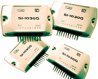
Amplifier circuit is very suitable for use in subwoofer amplifier system based on IC SI1030G. Amplfier has 30W output with 8 ohm impedance. Supply voltage required minimum of 12 volts and a maximum of up to 22 volts DC.

Component List :
R1 = 100K
R2 = 1R
C1 = 2.2uF
C2 = 100uFC3 = 47uF
C4 = 100nF
C5 = 10uF
C6 = 47uF
C7 = 100uF
IC = SI1020GL , SI1030G
Thursday, November 21, 2013
TDA9302 Vertical deflection output schematics
The TDA9302H is a monolithic integrated circuit in HEPTAWATTTM package. This is a high efficiency power amplifier for direct drive vertical rolls from the yokes of TV. This is intended to be used in Color and B & W television as well as in monitors and displays .

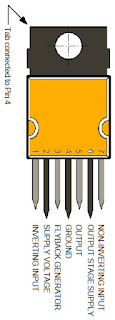
Supply Voltage pin 2 35V
Flyback peak voltage 60V
Voltage at pin 3 +Vs
Amplifier Input Voltage -0.5V
Deflection Output Current ± 1.8 A
Pin 3 DC Current at V5 < V2 100 mA
Total Power Dissipation at Tcase 90 °C
Storage and Junction Temperature – 40, +150°C
Part List :
Resistor
R1 = 12K
R2 = 10K
R3 = 27K
R4 = 12K
R5 = 1R
R6 = 330R
R7 = 1.5R
Ry = 5.9R
Capacitor
C1 = 680mF
C2 = 220uF
C3 = 220uF
C4 = 0.22uF
C5 = 1000uF
C6 = 4.7uF
Diode
D1 = BY252
IC = TDA9302H
Subscribe to:
Posts (Atom)