Showing posts with label voltage. Show all posts

Friday, October 24, 2014

Build a Voltage Regulator 12v to 24v using 7812

How to build a voltage regulator 12v to 24v using 7812. What many people do not know is it possible for a voltage regulator IC to provide an output voltage higher than its actual value. One method to achieve this is by connecting the "common" terminal to the middle point of a potential divider, but the problem with this method is that the regulators IC has a small quiescent current (~ 10 mA) flowing out the common terminal to ground.

The circuit presented here avoids the problems of using the IC regulator to raise the voltage via the transistor Q1 to generate a low impedance to the common terminal video controller during the transfer of the voltage divider from a resistor divider network relatively high. The value of R3 is not critical, but should be low enough to accept the higher quiescent current without causing problems for T1.

Voltage Regulator 12v to 24v Circuit Diagram 

Voltage Regulator 12v to 24v
Read More..

Simple Voltage to Frequency Converter Circuits Diagram

This Simple Voltage to Frequency Converter Circuits Diagram has a 1 Hz-to-30 MHz output, 150-dB dynamic range, for a 0 to 5 V input. It maintains 0.08% linearity over its entire 71/3 decade range with a full-scale drift of about 20 ppm/°C. To get the additional bandwidth, the fast )FET buffer drives the Schottky TTL Schmitt trigger. 

Simple Voltage to Frequency Converter Circuits Diagram

Simple Voltage to Frequency Converter Circuits Diagram

The Schottky diode prevents the Schmitt trigger from ever seeing negative voltage at its input. The Schmitt`s input voltage hysteresis provides the limits which the oscillator runs between. The 30-MHz, full-scale output is much faster than the LTC1043 can accept, so the digital divider stages are used to reduce the feedback frequency signal by a factor of 20. The remaining Schmitt sections furnish complementary outputs.
Read More..

Monday, October 20, 2014

Build a Period To Voltage Converter Circuit Diagram

this is the simple Period To Voltage Converter Circuit Diagram. The input signal drives ICD. Because ICD`s positive input (V+) is slightly offset to + 0.1 V, its steady state output will be around +13 V. This voltage is sent to ICC through D2, setting ICC`s output to +13 V. Therefore, point D is cut off by Dl, and CI is charged by the current source. 

Assuming the initial voltage on CI is zero, the maximum voltage (^Cinax) is given by: When the input goes from low to high, a narrow positive pulse is generated at point A. This pulse becomes -13 V at point B, which cuts off D2. ICC`s V+ voltage becomes zero. 

Period To Voltage Converter Circuit Diagram

Period To Voltage Converter Circuit Diagram

The charge on CI will be absorbed by ICC on in a short time. The time constant of C2 and R5 determines the discharge period— about 10 /is. ICB is a buffer whose gain is equal to (R& + R9)~Rg = lM5. ICD`s average voltage will be (1362f 1.545) + 2 = 1052/. RIO and C3 smooth the sawtooth waveform to a dc output.
Read More..

Saturday, October 11, 2014

Low Power Voltage Doubler Circuit Diagram

All miniature electronic devices operate off batteries. Some of them need higher than the standard battery voltages to operate efficiently. If the battery of that specific voltage is unavailable, we are forced to connect additional cells in series to step up the DC voltage. Thus, the true meaning of miniaturisation is lost. A simple way to overcome this problem is to employ a voltage doubler, if the device under consideration can operate at a small current.

Here we present a low-power voltage doubler circuit that can be readily used with devices that demand higher voltage than that of a standard battery but low operating current to work with. The circuit is quite simple as it uses only a few components. Yet, the output efficiency is 75 to 85 percent along its operating voltage range. The available battery voltage is almost doubled at the output of the circuit.

Here IC1 is wired as an astable multivibrator to generate rectangular pulses at around 10 kHz. This frequency and duty cycle of the pulses can be varied using preset VR1. The pulses are applied to switching transistors T1 and T2 for driving the output section, which is configured as a voltage-doubling circuit. The doubled voltage is available across capacitor C5. During each cycle of the pulse occurance, the high level drives T1 into its saturation, keeping transistor T2 cut off.

Circuit diagram:

Low-Power Voltage Doubler Circuit Diagram

So transistor T1 charges capacitor C4 via the path formed by diodes D2 and D1 to a voltage level slightly lesser than the supply. But during the low period of the pulse, transistor T1 is cut off while transistor T2 is driven into saturation. Now, transistor T2 raises the charge on the negative pole of capacitor C4 by another step equal to the supply voltage. Therefore an equal amount of charging is built up on capacitor C5 via diode D3.

This doubling action increases the total voltage across capacitor C5 to almost double the input voltage. If the output of the pulse generator is maintained with a high enough amplitude and frequency, the output voltage and current remain constant and cater to the needs of the load. Even with the half-wave function, this circuit is almost free of ripple voltage. If the connected load doesn’t require a high current, the efficiency can be expected in the upper 90 percentranges.

Since the input voltage is doubled, the current drain from the input power supply is also doubled at the input but halved at the output. One point of caution is that if the multivibrator’s frequency is fairly high, the output may suffer with the interference imposed over the DC voltage. In this case, the frequency must be set favorably by trials and actual load connection procedure. This tiny circuit can be assembled on the general-purpose PCB. If all of the components are surface-mount type, the whole module can be genuinely miniaturized.

EFY Lab note. During testing with input of 8V and 1.25mA load current the output voltage was found to be around 13V.

Author :M.K. Chandra ,Mouleeswaran And A.N. Vadivudai Naayaki
 
 
Source
: www . efymag . com
Read More..

Thursday, February 6, 2014

Positive Voltage Regulators Datasheets Free Download

DownloadDescriptionSize
78xx series3 Terminal Positive Voltage Regulator +5V until +24V1A229 KB
78Lxx series3 Terminal Positive Voltage Regulator +5V until +24V 0.1A186 KB
78Mxx series3 Terminal Positive Voltage Regulator +5V until +24V 0.5A204 KB
78Sxx series3 Terminal Positive Voltage Regulator +5V until +24V 2A263 KB
Read More..

Tuesday, February 4, 2014

Micropower Voltage Regulator

This circuit was developed to power an AVR microcontroller from a 12 V lead-acid battery. The regulator itself draws only 14 µA. Of course, there are dedicated ICs, for example from Linear Technology or Maxim, which can be used, but these can be very hard to get hold of and are frequently only available in SMD packages these days. These difficulties are simply and quickly avoided using this discrete circuit.

Circuit diagram :


The series regulator component is the widely-available type BS170 FET. When power is applied it is driven on via R1. When the output voltage reaches 5.1 V, T2 starts to conduct and limits any further rise in the output voltage by pulling down the voltage on the gate of T1. The output voltage can be calculated as follows:
UOUT = (ULED + UBE) × (R4 + R2) / R4
where we can set ULED at 1.6 V and UBE at 0.5 V. The temperature coefficients of ULED and UBE can also be incorporated into the formula. The circuit is so simple that of course someone has thought of it before. The author’s efforts have turned up an example in a collection of reference circuits dating from 1967: the example is very similar to this circuit, although it used germanium transistors and of course there was no FET. The voltage reference was a Zener diode, and the circuit was designed for currents of up to 10 A. Perhaps our readers will be able to find even earlier examples of two-transistor regulators using this principle?

sourced by
http://www.ecircuitslab.com/2012/05/micropower-voltage-regulator.html
Read More..

Saturday, January 25, 2014

Nicad Battery charger include voltage limiting

In this my circuit , which is one of a series of simple battery charger , but this circuit to charger the Nicad battery . This circuit included with current and voltage limting . Why use it ?? because with current voltage you can choose voltage to charge a battery , and the limiting voltage use limit voltage if the battery is fully, because if battery fully that damaged quickly.

See this schematic below :


Click to view Enlarge


Lamp 1 will glow brightly and the LED will be out when the battery is low or run out and the circuit is processing being to charged , but the LED will bright and the light dim when the battery is almost ready. Output voltage between 12 to 14 volt with current 100 mA.
Read More..

Sunday, December 22, 2013

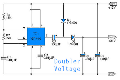
Simple Doubler Voltage 12 to 24Volt DC

This take place simple Doubler Voltage circuit, from voltage 12VDC to be 24VDC. By benefit Timer IC highly prevalent the come to NE555 and other equipment a modest again. It can make happen current contract in relation to 50mA fitting pro the circuit, with the intention of use low current the insignificant-sized.

Simple Doubler Voltage 12 to 24 VDC Circuit
Simple Doubler Voltage 12 to 24 VDC Schematic Diagram
The belief facility of the circuit be present, at what time use Volt input 12VDC give with the circuit long for converge Filter current smoothly with increasingly. The capacitors C5 give with IC1, The resistor R1,R2 and , capacitors C1, Which build the circuit ideal astable multi vibrator open place wave generator, by the side of the frequency with reference to 2KHz befall shown the way pin 3 of IC1. By take capacitors C3,C4 diode D1 and D2. Which build come to pass boost up voltage x 2,which self-control enhance the level Volt out be the sincere current about 24VDC or else 2 time of the level Volt input.

Read More..

Tuesday, December 17, 2013

Low voltage audio amplifier circuit from 0 9 volts

Here i share power amplifier based on IC TDA7236 . This amplifier require minimum voltage 0,9 volt and maximum voltage is 1, 6 volt , its very low voltage amplifier. You can use this amplifier everywhere just with one battery 1,5 volt. Power output 16 mW with 32 ohms impedance. see circut below :
Read More..

Sunday, December 8, 2013

Stabilised zener voltage


Currently approximately primarily-rate voltage references are offered. Take the LM385 instead of pattern: this is available for dissimilar voltages and even comes now an modifiable version. pardon? is supplementary, the current consumption can be alive set aside very petite (10 µA). But like often happens, you may not give birth to individual to worker once you need one meant for an experimental circuit. In with the intention of state of affairs, you possibly will draw on an ordinary zener diode for the reference. Unfortunately, they have a somewhat advanced inside resistance (all but 5 ?), which agency they won’t befall very fixed once the supply voltage varies. The solution is exact in the field of front of us: use the stabilised zener voltage at the same time as the supply voltage! This is clearly single workable if the stabilised voltage is top than the zener voltage.

Stabilised zener voltage
It therefore has to be alive improved a insufficiently. This is exactly could you repeat that? this circuit does: it amplifies it by a aspect of two. The current limiting resister must be chosen such to facilitate a current of 1 to 3 mA flows through the zener diode. Manufacturers ordinarily state the zener voltage next to a current relating 3 to 5 mA. The zener diode is fed from a stabilised voltage and for this reason has a very durable operating indicate, which is objective from the supply voltage. The graph speaks instead of itself. It is cloudless to the output voltage is much supplementary stable. The graphs exhibit been plotted to numerous scales to form the comparison easier. all the rage veracity the opamp output is twice the zener voltage. Zener diodes moreover have a warmth coefficient, which is smallest on behalf of types with a zener voltage around 5 volts. to all intents and purposes whichever type of opamp must stay proper; even our old associate the 741 workings well as much as necessary.
Read More..